Method and system of robot fork calibration and wafer pick-and-place

a robot fork and wafer technology, applied in the field of mechanical equipment manufacturing, can solve the problems of irreparable losses such as damage to the wafer or equipment, and achieve the effects of avoiding accidental collision between reducing the risk of damage to the fork and the wafer, and improving the safety of wafer handling

Active Publication Date: 2018-08-21
BEIJING NAURA MICROELECTRONICS EQUIP CO LTD
View PDF5 Cites 1 Cited by
  • Summary
  • Abstract
  • Description
  • Claims
  • Application Information

AI Technical Summary

Benefits of technology

[0007]In order to overcome the drawbacks mentioned above, the present invention provides a robot fork calibration method and system, which can fast and accurate detect the height and levelness state of the robot fork, so as to ensure a safe wafer pick-and-place operation.
[0016]According to the present invention, a reference coordinate system is established in which a detection point on an horizontal upper surface of the robot base station is set as a zero point and the horizontal upper surface is set as the XOY plane, and the tilted angle of the fork as well as the fork height can be calculated according to the detection by the lower sensors disposed on the bottom surface of the fork during the motion of the robot, so as to monitor the fork pose and calibrate the height and levelness of the fork in time. Therefore, wafer damages due to unexpected collision between the fork and the wafer can be avoided, and wafer handling safety can be improved. Furthermore, during the actual wafer pick-and-place operation, the pose of the target wafer can be recognized on the basis of the calibrated robot fork, so as to avoid wafer slippery or wafer collision with the fork.

Problems solved by technology

However, factors such as robot fork rotation or positional offset may cause collision of the robot fork with the wafer or wafer carrier when the robot performs the pick-and-place operation, resulting in irreparable losses such as damages to the wafer or equipment.

Method used


Image

  • Method and system of robot fork calibration and wafer pick-and-place
  • Method and system of robot fork calibration and wafer pick-and-place
  • Method and system of robot fork calibration and wafer pick-and-place

Examples


Embodiment Construction

[0025]Reference will now be made in detail to the present preferred embodiments to provide a further understanding of the invention. The specific embodiments and the accompanying drawings discussed are merely illustrative of specific ways to make and use the invention, and do not limit the scope of the invention or the appended claims.

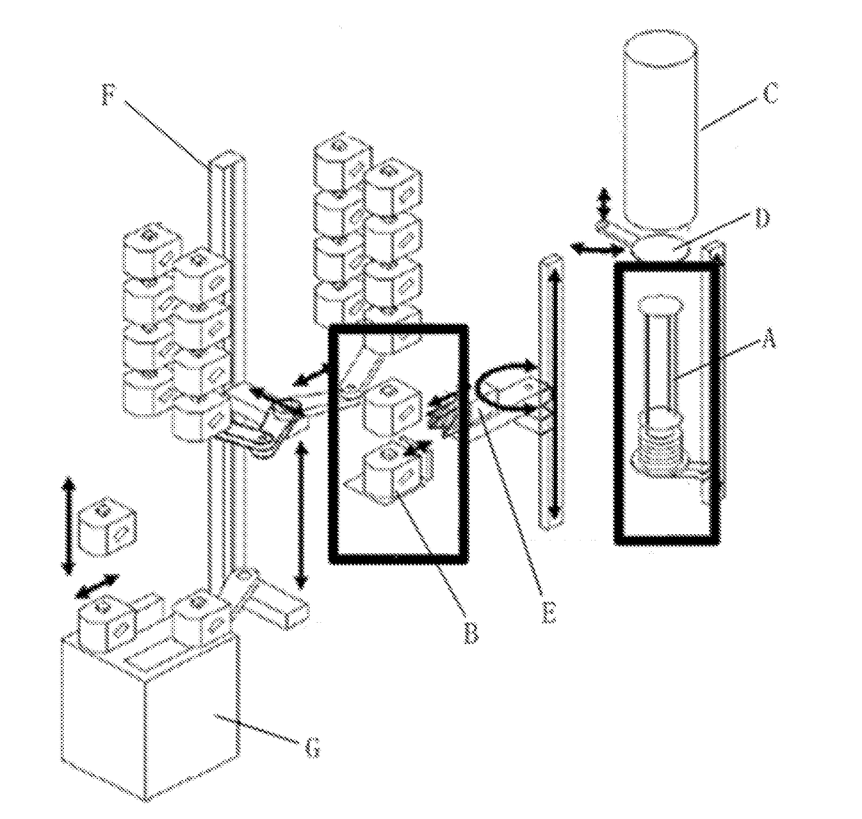
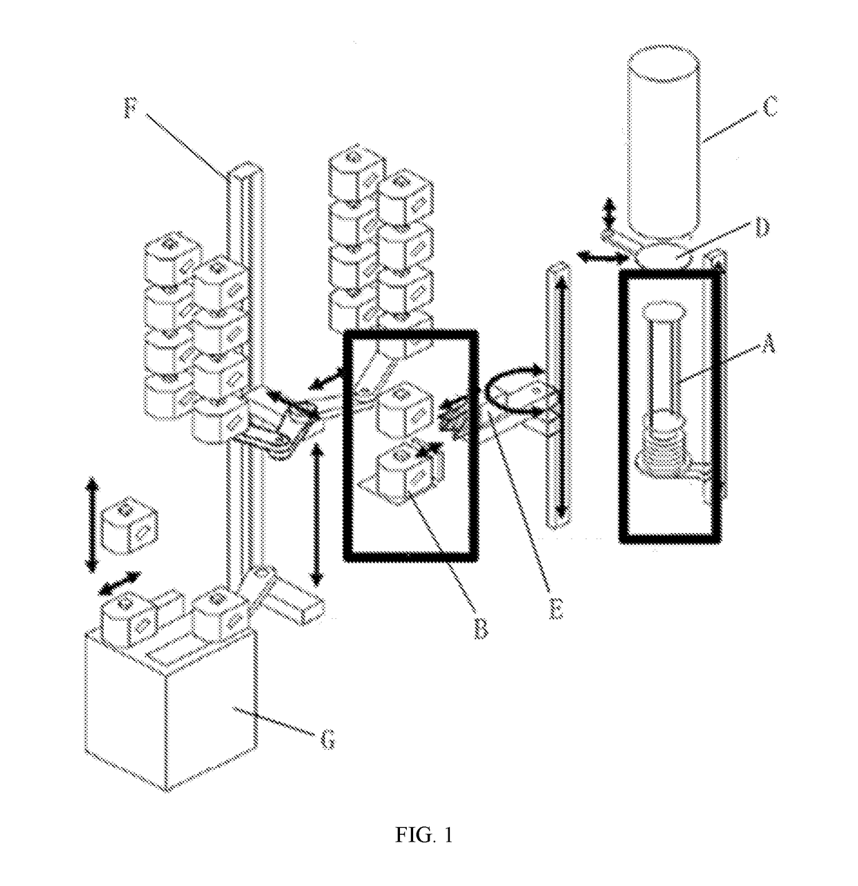
[0026]The semiconductor equipment of the present invention includes a wafer carrier which supports multiple wafers and a robot which performs the wafer pick-and-up operation. The wafer carrier has supporters on which the wafers are horizontally positioned in a vertical stack. As shown in FIG. 1, in an embodiment of the present invention, the wafer carrier can be a front-opening unified pod (FOUP) B which stores the wafers. It can also be a wafer boat A which loads the wafers into a reaction chamber C. The semiconductor equipment further has a FOUP holder F for holding the FOUPs B, which is connected to a pedestal G. During wafer handling, the robot E p...


PUM


Abstract

A robot fork calibration method and system is provided. At least three non-linear arranged lower sensors are provided on a bottom surface of the fork to detect distances to a fixed detection point. The fixed detection point and a horizontal plane of the detection point define a reference coordinate system. Spatial coordinates of the lower sensors in the reference coordinate system are calculated and a plane equation as well as a tilted angle of the fork are obtained according to the spatial coordinates. Therefore, the height of the fork can be calibrated according to the Z axis coordinates of the lower sensors and the levelness of the fork can be calibrated according to the tilted angle.

Description

CROSS-REFERENCE TO RELATED APPLICATION[0001]The application is related to and claims the priority benefit of Chinese Patent Application Serial No. 201511021465.6, filed Dec. 31, 2015, Chinese Patent Application Serial No. 201511022412.6, filed Dec. 31, 2015, and Chinese Patent Application Serial No. 201511023889.6, filed Dec. 31, 2015; the entirety of each of the above-mentioned patent applications is hereby incorporated by reference herein and made a part of the specification.FIELD OF THE INVENTION[0002]The present invention generally relates to the field of semiconductor manufacturing equipment, more particularly, to methods and systems of robot fork calibration and wafer pick-and-place.BACKGROUND OF THE INVENTION[0003]Safe wafer pick-and-place is a very important technical indicator for integrated circuit production lines. Generally, the breakage rate of wafers due to wafer handling equipment in the course of production should be less than 0.001%. Compared with a single-wafer pro...

Claims


Application Information

Patent Timeline
Patent Type & Authority Patents(United States)
IPC IPC(8): G05B19/04H01L21/677H01L21/67H01L21/68B25J9/16
CPCH01L21/67766H01L21/68H01L21/67259B25J9/1692H01L21/67265H01L21/67778H01L21/68707
Inventor XU, DONG
Owner BEIJING NAURA MICROELECTRONICS EQUIP CO LTD
Why Eureka
Try Eureka