Ultra high density display having high aperture ratio
a high-density display and aperture ratio technology, applied in the direction of instruments, organic semiconductor devices, semiconductor devices, etc., can solve the problems of degrading video quality, achieve the effect of maximizing aperture ratio, ensuring quality, and keeping video quality in superior quality
- Summary
- Abstract
- Description
- Claims
- Application Information
AI Technical Summary
Benefits of technology
Problems solved by technology
Method used
Image
Examples
first embodiment
[0056]Referring to FIG. 6, we will explain about the first embodiment of the present disclosure. FIG. 6 is a plane view illustrating a structure of one pixel in an organic light emitting diode display having a compensation element according to the first embodiment of the present disclosure.
[0057]The organic light emitting diode display according to the first embodiment of the present disclosure comprises a sensing line REF, a data line DL, a driving current line VDD, a horizontal sensing line REFh, a horizontal current line VDDh and a scan line SL on a substrate SUB. These lines define a pixel area. In detail, a unit pixel area is defined as an area surrounded by two neighboring horizontal sensing lines REFh, one data line DL and one driving current line VDD.
[0058]The scan line SL, the horizontal sensing line REFh and the horizontal current line VDDh are running in horizontal direction on the substrate SUB. The data line DL, the driving current line VDD and the sensing line REF are ...
second embodiment
[0072]Hereinafter, referring to FIG. 7 we will explain about an organic light emitting diode display according to the second embodiment in which the organic light emitting diode OLE is disconnected from the thin film transistor. FIG. 7 is a plane view illustrating a structure of one pixel in an ultra high density organic light emitting diode display having a bottle neck portion for darkening a defected pixel according to the second embodiment of the present disclosure.
[0073]The organic light emitting diode display according to the second embodiment is very similar with the display according to the first embodiment. The same or similar elements with the first embodiment will not be duplicated. The main difference point is on the structure of the anode electrode ANO.
[0074]The anode electrode ANO according to the second embodiment further includes an anode bottle neck part PCN at the lower side of the pixel area. The anode bottle neck part PCN is formed by narrowing the width of some p...
third embodiment
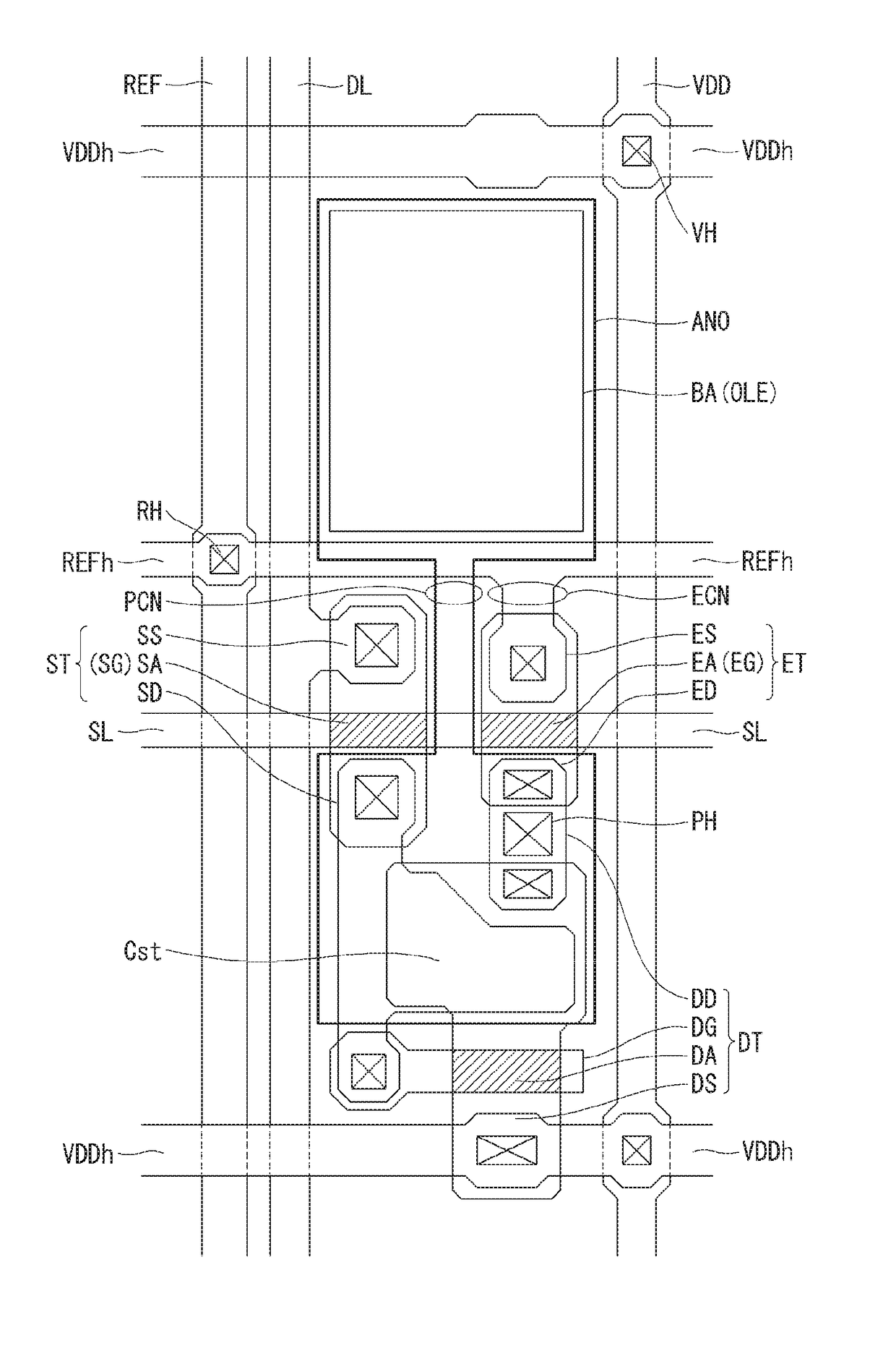
[0077]Hereinafter, in the third embodiment, we will suggest unique structure of the organic light emitting diode display including the bottle neck part for darkening the defected pixel and ensuring the maximized aperture ratio. FIG. 8 is a plane view illustrating a structure of one pixel in an ultra high density organic light emitting diode display having a bottle neck portion for darkening a defected pixel according to the third embodiment of the present disclosure.
[0078]The organic light emitting diode display according to the third embodiment of the present disclosure comprises a sensing line REF, a data line DL, a driving current line VDD, a horizontal sensing line REFh, a horizontal current line VDDh and a scan line SL. The pixel is defined by these lines. For example, a space surrounded by two neighboring horizontal current line VDDh, the data line DL and the driving current line VDD is defined as the unit pixel area.
[0079]The scan line SL, the horizontal sensing line REFh and...
PUM
 Abstract
Description
Claims
Application Information


