Imaging device, method for operating the same, module, and electronic device

a technology of imaging device and module, applied in the field of imaging device, can solve the problems of difficult imaging with a global shutter system, difficult to store the obtained imaging data in all pixels, etc., and achieve the effect of reducing the size of pixels

Active Publication Date: 2018-10-02
SEMICON ENERGY LAB CO LTD
View PDF63 Cites 0 Cited by
  • Summary
  • Abstract
  • Description
  • Claims
  • Application Information

AI Technical Summary

Benefits of technology

[0013]As a method for reducing the sizes of pixels included in an imaging device, a method in which transistors are shared by pixels is given.
[0014]By imaging with a global shutter system, simultaneousness of imaging in all the pixels in the imaging device can be secured, and an image with little distortion can be easily obtained even when the object moves.
[0016]An object of one embodiment of the present invention is to provide an imaging device which can perform imaging with a global shutter system even when transistors are shared by pixels. Another object of one embodiment of the present invention is to provide an imaging device which can capture an image with little distortion even when the object moves.
[0017]Another object of one embodiment of the present invention is to provide an imaging device which can take a high-resolution image. Another object of one embodiment of the present invention is to provide a small-sized imaging device. Another object of one embodiment of the present invention is to provide an imaging device with reduced power consumption. Another object of one embodiment of the present invention is to provide an imaging device that is suitable for high-speed operation. Another object of one embodiment of the present invention is to provide an imaging device including a transistor with a high on-state current. Another object of one embodiment of the present invention is to provide an imaging device including a transistor with a low off-state current. Another object of one embodiment of the present invention is to provide an imaging device including a transistor to which a high potential can be applied. Another object of one embodiment of the present invention is to provide an imaging device with a large dynamic range. Another object of one embodiment of the present invention is to provide an imaging device with a long retention period for imaging data. Another object of one embodiment of the present invention is to provide an imaging device which can be used at a wide range of temperatures. Another object of one embodiment of the present invention is to provide an imaging device which can obtain imaging data with less noise. Another object of one embodiment of the present invention is to provide an imaging device with high optical sensitivity. Another object of one embodiment of the present invention is to provide an inexpensive imaging device. Another object of one embodiment of the present invention is to provide an imaging device with high reliability.
[0028]According to one embodiment of the present invention, an imaging device which can perform imaging with a global shutter system even when transistors are shared by pixels can be provided. An imaging device which can capture an image with little distortion even when the object moves can be provided.
[0029]An imaging device which can take a high-resolution image can be provided. A small-sized imaging device can be provided. An imaging device with reduced power consumption can be provided. An imaging device that is suitable for high-speed operation can be provided. An imaging device including a transistor with a high on-state current can be provided. An imaging device including a transistor with a low off-state current can be provided. An imaging device including a transistor to which a high potential can be applied can be provided. An imaging device with a large dynamic range can be provided. An imaging device with a long retention period for imaging data can be provided. An imaging device which can be used at a wide range of temperatures can be provided. An imaging device which can obtain imaging data with less noise can be provided. An imaging device with high optical sensitivity can be provided. An inexpensive imaging device can be provided. An imaging device with high reliability can be provided.

Problems solved by technology

Meanwhile, in the case where transistors are shared by a plurality of pixels in a conventional imaging device, it is difficult to store the obtained imaging data in all the pixels.
Accordingly, imaging with a global shutter system is difficult.

Method used


Image

  • Imaging device, method for operating the same, module, and electronic device
  • Imaging device, method for operating the same, module, and electronic device
  • Imaging device, method for operating the same, module, and electronic device

Examples


embodiment 1

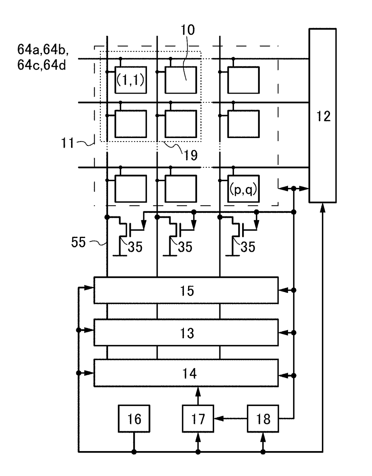
[0103]An imaging device of one embodiment of the present invention is described with reference to drawings. Note that in this specification and the like, an imaging device refers to any device that has an imaging function. The imaging device also indicates a circuit having a function of imaging or an entire system including such a circuit.

[0104]One embodiment of the present invention relates to an imaging device which can perform imaging with a global shutter system and in which transistors are shared by a plurality of pixels. As described in Embodiment 3 later, a photoelectric conversion element included in the imaging device of one embodiment of the present invention is stacked over another element, whereby it becomes unnecessary to electrically connect a source or a drain of a transistor having a function of selecting a pixel to a source or a drain of an amplifier transistor. As a result, the number of transistors per pixel can be reduced. In this manner, an imaging device which ...

embodiment 2

[0198]In this embodiment, a variation example of the pixel 10 of the imaging device of one embodiment is described with reference to drawings.

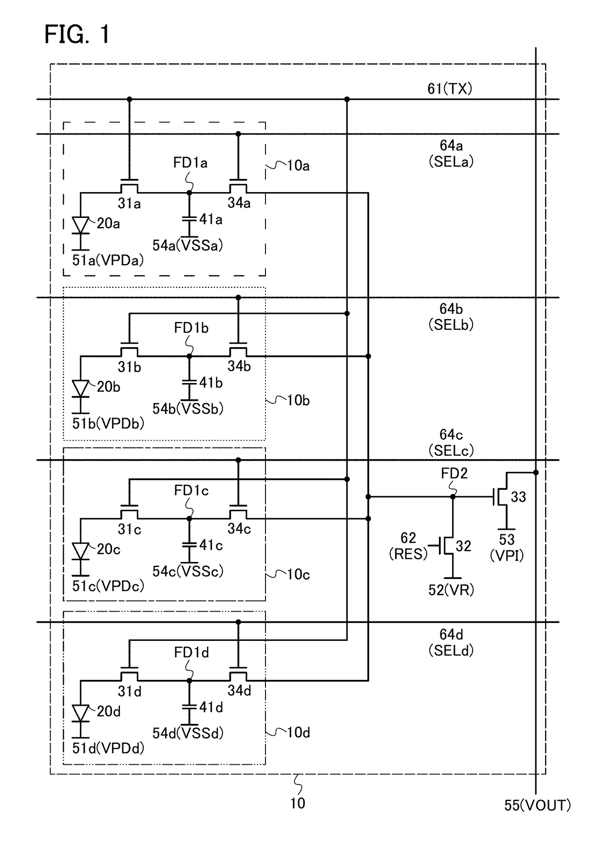
[0199]FIG. 7 shows a configuration in which the transistors 31a to 31d, the transistor 32, and the transistors 34a to 34d included in the pixel 10 shown in FIG. 1 are replaced with switches. Instead of the transistors, other elements can be used as long as they have a switching function. Note that some of the transistors 31a to 31d, the transistor 32, and the transistors 34a to 34d may be transistors and the other thereof may be other elements having a switching function.

[0200]FIG. 8 shows a configuration in which the transistor 33 included in the pixel 10 with the configuration shown in FIG. 1 is a p-ch transistor. FIG. 4 can be referred to for the operation of the pixel 10 with this configuration. Note that the potentials of the wiring 52 (VR) and the wirings 54a (VSSa) to 54d (VSSd) are set to an H level, and the potentials of the wirings 5...

embodiment 3

[0213]In this embodiment, specific configuration examples of the imaging device of one embodiment of the present invention are described below with reference to drawings.

[0214]FIG. 16A illustrates an example of a cross-sectional view of the imaging device of one embodiment of the present invention to illustrate a specific connection between the photoelectric conversion element 20a, the transistor 31a, the transistor 32, and the capacitor 41a which are included in the pixel 10a in FIG. 1. Note that the transistors 32 and 33 are not illustrated in FIG. 16A. The transistors 31a, 32, 33, and 34a and the capacitor 41a can be provided in a layer 1100, and the photoelectric conversion element 20a can be provided in a layer 1200.

[0215]The photoelectric conversion element 20a includes a photoelectric conversion layer 21, a light-transmitting conductive layer 22, and an electrode 26. The light-transmitting conductive layer 22 is electrically connected to one of the source and the drain of the...


PUM


Abstract

An imaging device which can perform imaging with a global shutter system and in which transistors are shared by pixels is provided. The imaging device includes first and second photoelectric conversion elements and first to sixth transistors. Active layers of the first to fourth transistors each include an oxide semiconductor. The imaging device has a configuration in which a reset transistor and an amplifier transistor are shared by a plurality of pixels and can perform imaging with a global shutter system. In addition, the imaging device can be used as a high-speed camera.

Description

BACKGROUND OF THE INVENTION[0001]1. Field of the Invention[0002]One embodiment of the present invention relates to an imaging device and an operation method thereof.[0003]Note that one embodiment of the present invention is not limited to the above technical field. The technical field of one embodiment of the invention disclosed in this specification and the like relates to an object, a method, or a manufacturing method. Furthermore, one embodiment of the present invention relates to a process, a machine, manufacture, or a composition of matter. Specifically, examples of the technical field of one embodiment of the present invention disclosed in this specification include a semiconductor device, a display device, a liquid crystal display device, a light-emitting device, a lighting device, a power storage device, a memory device, an imaging device, a method for operating any of them, and a method for manufacturing any of them.[0004]In this specification and the like, a semiconductor ...

Claims


Application Information

Patent Timeline
Patent Type & Authority Patents(United States)
IPC IPC(8): H01L29/10H04N5/3745H01L27/146
CPCH01L27/14616H01L27/1462H01L27/14607H01L27/14627H04N5/37457H01L27/14609H01L27/14696H01L27/14641H04N25/778
Inventor IKEDA, TAKAYUKI
Owner SEMICON ENERGY LAB CO LTD
Why Eureka
Try Eureka