Display substrate and manufacturing method thereof, and bistable liquid crystal display panel
a liquid crystal display and substrate technology, applied in the direction of thin material processing, instruments, chemistry apparatus and processes, etc., can solve the problems of poor display effect, low contrast, high power consumption, etc., and achieve low transmittance, high transmittance, and high transmittance
- Summary
- Abstract
- Description
- Claims
- Application Information
AI Technical Summary
Benefits of technology
Problems solved by technology
Method used
Image

Examples
embodiment 1
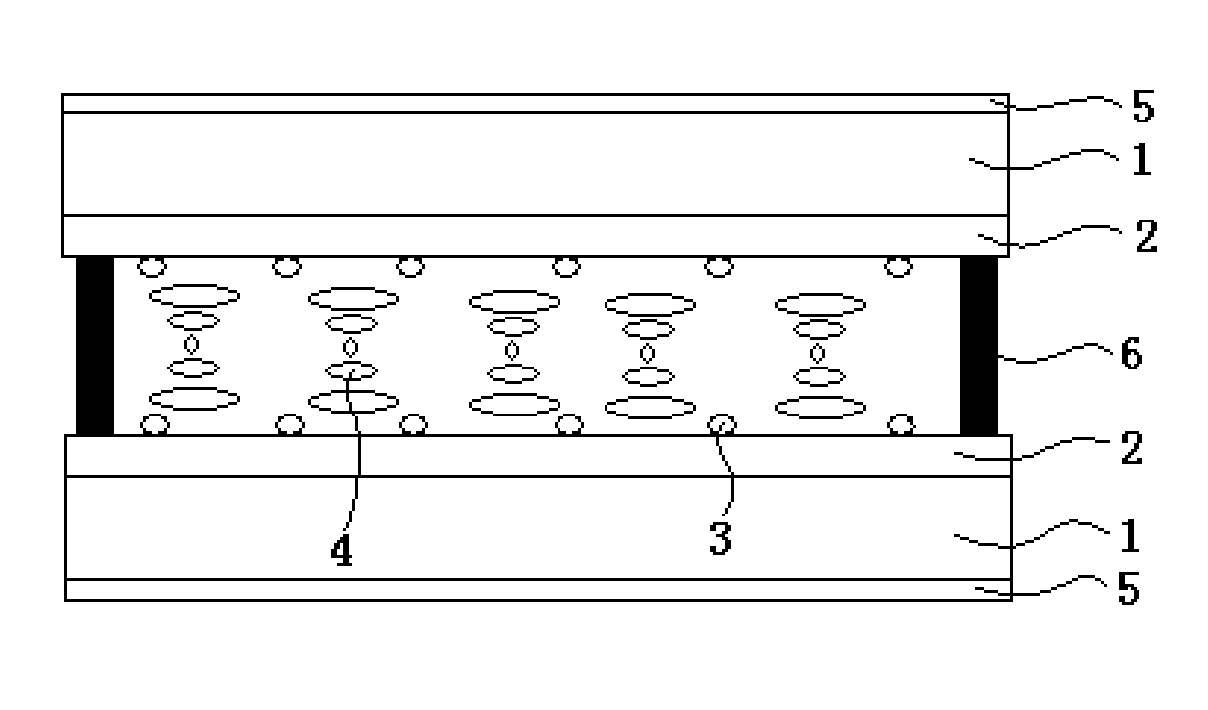
[0046]As shown in FIG. 1, the present embodiment provides a display substrate and a manufacturing method thereof.
[0047]The display substrate comprises a base substrate 1, on which conventional display structures (for example, a driving array, a common electrode, a pixel electrode, and color filters) are provided, as these display structures are known and various, detail description thereof will be omitted here.
[0048]A biphenyl polymer layer 2 (that is, a polymer layer polymerized by monomers containing biphenyl group) is provided on the base substrate 1, the biphenyl polymer layer 2 comprises a skeleton and meshes formed in the skeleton, and the meshes are uniformly distributed in the skeleton.
[0049]The liquid crystal molecules may be inserted into the meshes of the biphenyl polymer layer 2 when they contact with the biphenyl polymer layer 2, since the meshes are uniformly distributed in the skeleton, the liquid crystal molecules contacting with the biphenyl polymer layer 2 are dist...
embodiment 2
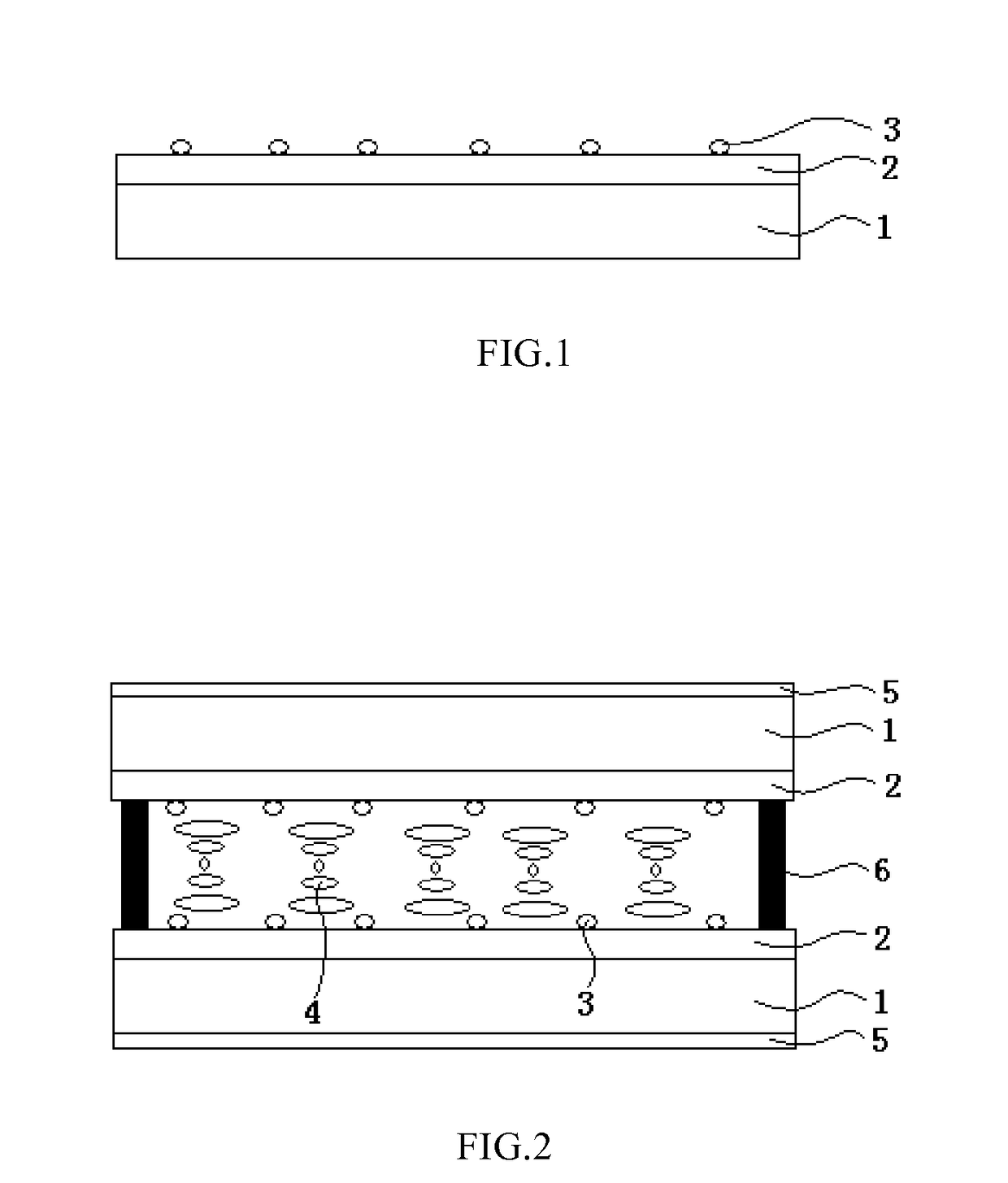
[0088]As shown in FIG. 2, the present embodiment provides a bistable liquid crystal display panel comprising a first display substrate and a second display substrate which are aligned and assembled, and a liquid crystal layer provided between the first display substrate and the second display substrate, wherein
[0089]the first display substrate is the above display substrate, and a biphenyl polymer layer 2 of the first display substrate faces the liquid crystal layer (that is, the biphenyl polymer layer 2 of the first display substrate contacts the liquid crystal layer),
[0090]and / or
[0091]the second display substrate is the above display substrate, and a biphenyl polymer layer 2 of the second display substrate faces the liquid crystal layer (that is, the biphenyl polymer layer 2 of the second display substrate contacts the liquid crystal layer).
[0092]That is to say, at least one of the first display substrate and the second display substrate of the bistable liquid crystal display pane...
PUM
| Property | Measurement | Unit |
|---|---|---|
| aperture size | aaaaa | aaaaa |
| thickness | aaaaa | aaaaa |
| grain size | aaaaa | aaaaa |
Abstract
Description
Claims
Application Information