Supercharge Your Innovation With Domain-Expert AI Agents!

Thin film transistor substrate

a technology of thin film transistors and substrates, applied in the direction of electrical equipment, semiconductor devices, instruments, etc., can solve the problems of affecting the initial characteristics and reliability of tfts by hydrogen in the channel layer, and achieve the effect of excellent reliability

Active Publication Date: 2018-10-16
TRIVALE TECH
View PDF52 Cites 0 Cited by
  • Summary
  • Abstract
  • Description
  • Claims
  • Application Information

AI Technical Summary

Benefits of technology

The invention relates to a thin film transistor substrate with a gate electrode that can absorb hydrogen during manufacturing or operation, preventing it from affecting the semiconductor layer or causing variations in the transistor's characteristics. This results in a thin film transistor with improved reliability and consistent performance.

Problems solved by technology

Thus, hydrogen in the channel layer affects initial characteristics and reliability of a TFT.

Method used


Image

  • Thin film transistor substrate
  • Thin film transistor substrate
  • Thin film transistor substrate

Examples


first embodiment

[0049]Descriptions will be made assuming that a TFT substrate according to a first embodiment is an active matrix substrate on which a thin film transistor (Thin Film Transistor) is used as a switching device.

[0050]

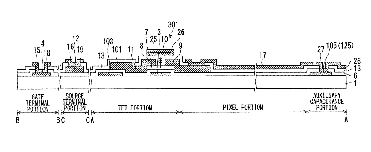
[0051]FIG. 1 is a plan view that schematically describes configuration of overall of a TFT substrate of the first embodiment according to the present invention, and takes a TFT substrate for an LCD as an example here.

[0052]A TFT substrate 200 illustrated in FIG. 1 is a TFT array substrate on which pixel TFTs 201 are arranged in a matrix, and is roughly divided into a display region 202 and a bezel region 203 provided so as to enclose the display region 202.

[0053]In the display region 202, a plurality of gate wires (scanning signal lines) 103, a plurality of auxiliary capacitance wires 105, and a plurality of source wires (display signal lines) 101 are arranged, the plurality of gate wires 103 are arranged in parallel with each other, and the plurality of source wires 101 ...

second embodiment

[0163]

[0164]FIG. 23 is a plan view that schematically describes configuration of overall of a TFT substrate of a second embodiment according to the present invention, and note that the same configuration as in the TFT substrate described with reference to FIG. 1 is denoted with the same symbol, and duplicate description will be omitted.

[0165]A TFT substrate 300 illustrated in FIG. 23 is a TFT array substrate on which pixel TFTs 301 are arranged in a matrix.

[0166]In FIG. 23, part of pixels 304 is illustrated with configuration thereof enlarged, and at least one pixel TFT 301 is disposed within the pixel 304. The pixel TFT 301 is disposed near an interportion of a source wire 101 and a gate wire 103, a gate electrode of the pixel TFT 301 is connected to the gate wire 103, a source electrode of a pixel TFT 301 is connected to the source wire 101, and a drain electrode of the pixel TFT 301 is connected to a transmissive pixel electrode 17.

[0167]In addition, auxiliary capacitance 209 is ...


PUM

PropertyMeasurementUnit
threshold voltageaaaaaaaaaa
drain currentaaaaaaaaaa
thicknessaaaaaaaaaa

Abstract

A thin film transistor substrate includes: a plurality of pixels arranged in a matrix, each of the pixels including: a thin film transistor including: a gate electrode made of a metal and disposed on the substrate; a gate insulating film covering at least the gate electrode; a semiconductor layer including an oxide semiconductor provided at a position facing the gate electrode with the gate insulating film interposed therebetween; a source electrode and a drain electrode in contact with the semiconductor layer; and an interlayer insulating film provided on at least the semiconductor layer, the source electrode, and the drain electrode; and a pixel electrode electrically connected to the drain electrode. The gate electrode has hydrogen occlusion capability of 2.5×10²⁰ to 2×10²² atoms / cm3, and the semiconductor layer has a hydrogen concentration of 1×10¹⁶ atoms / cm3 or less.

Description

TECHNICAL FIELD[0001]The present invention relates to a thin film transistor substrate used for a liquid crystal display device and the like.BACKGROUND ART[0002]An electro-optic device such as a liquid crystal display (Liquid Crystal Display: hereinafter referred to as “LCD”) includes a thin film transistor substrate (hereinafter referred to as “TFT substrate”) using a thin film transistor (Thin Film Transistor: hereinafter referred to as “TFT”) as a switching device.[0003]A semiconductor device such as a TFT has a characteristic of low power consumption and a thin profile. Therefore, by utilizing such a characteristic of the semiconductor device, application to a flat panel display has been made, replacing a CRT (Cathode Ray Tube).[0004]In an LCD which is one example of a flat panel display, generally, a liquid crystal layer is provided between a TFT substrate and a counter substrate. On the TFT substrate, TFTs are arranged, for example, in a matrix. Polarizing plates are provided ...

Claims


Application Information

Patent Timeline
Patent Type & Authority Patents(United States)
IPC IPC(8): H01L29/786H01L27/12G02F1/1368G02F1/1333
CPCH01L29/7869G02F1/1368H01L27/124H01L27/1225G02F1/133345G02F2201/123H01L29/4908H01L27/1255
Inventor IMAZAWA, TAKASHIFUJINO, TOSHIAKIMOTOYA, TSUKASA
Owner TRIVALE TECH
Features
  • R&D
  • Intellectual Property
  • Life Sciences
  • Materials
  • Tech Scout
  • Unparalleled Data Quality
  • Higher Quality Content
  • 60% Fewer Hallucinations
Learn More