Gate line drive circuit and display device having the same

a technology of gate line drive and display device, which is applied in the field of display panel, can solve the problems of gate line drive circuit breakdown and inability to properly transmit output signal gn, and achieve the effects of improving the display quality of the display panel, facilitating the adjustment of the duty cycle of output signal, and improving the accuracy of timing control of output signal

Active Publication Date: 2018-10-30
FOCALTECH SYST CO LTD
View PDF4 Cites 0 Cited by
  • Summary
  • Abstract
  • Description
  • Claims
  • Application Information

AI Technical Summary

Benefits of technology

[0008]The aspect of the present disclosure is to provide a gate line drive circuit and a display device having the same. In the present disclosure, driving of the gate line is separate and independent from control of the next-stage gate line drive circuit so as to prevent the output signal from waveform distortion in multi-stage transmission. Since the gate line can be driven separately and independently from control of the next-stage gate line drive circuit, it is easier to adjust the duty cycle of the output signal and, in comparison with the prior art, the accuracy of timing control for the output signal can be increased so as to further improve the display quality of the display panel. Moreover, in the present disclosure, the transistor drives the gate line with current larger than that in the prior art, and thus the rising time or the falling time of the present disclosure is shorter than that of the prior art.

Problems solved by technology

As a result, the output signal Gn cannot be properly transmitted, and thus the gate line drive circuit breaks down.

Method used


Image

  • Gate line drive circuit and display device having the same
  • Gate line drive circuit and display device having the same
  • Gate line drive circuit and display device having the same

Examples


first embodiment

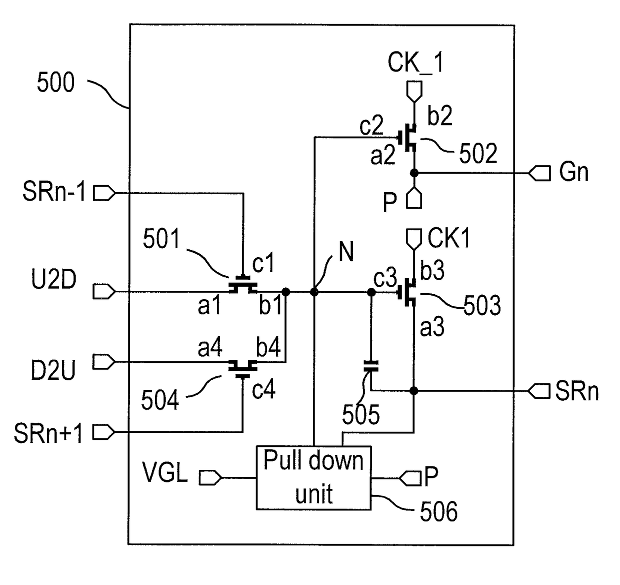
[0025]FIG. 5 is schematic diagram of the gate line drive circuit 500 in accordance with the present disclosure. The gate line drive circuit 500 includes a first transistor 501, a second transistor 502, a third transistor 503, a fourth transistor 504, a boosting capacitor 505, and a pull-down unit 506.

[0026]The first transistor 501 includes a control terminal c1 connected to a charge / discharge control signal SRn−1 of a previous-stage gate line drive circuit, a first terminal a1 connected to a charge high voltage U2D, and a second terminal b1 connected to a control node N.

[0027]The second transistor 502 includes a control terminal c2 connected to the control node N, a first terminal a2 connected to a gate line Gn, and a second terminal b2 connected a first clock signal CK_1. In the first embodiment of the present disclosure, the symbol Gn may represent a physical element, i.e. the gate line, or a signal on the physical element, i.e. the signal on the gate line. Such symbol representat...

second embodiment

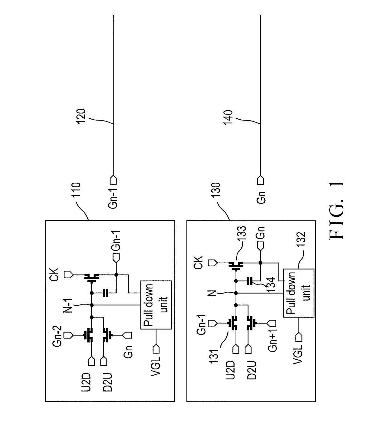
[0041]In FIG. 10, there are two nodes labeled with P, indicating that the two nodes are electrically connected together, which is a habitual practice in electronic circuit drawings and thus a detailed description therefor is deemed unnecessary. FIG. 11 is a timing diagram for the gate line drive circuit 500 shown in FIG. 10 in accordance with the present disclosure. The operation of FIG. 11 can be known with reference to FIG. 6 and its related description, and thus a detailed description therefor is deemed unnecessary.

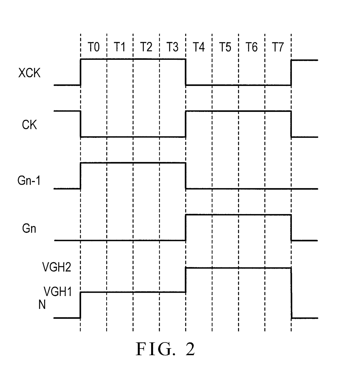
[0042]From the comparison of FIG. 6 with FIG. 3, when the duration of the output signal Gn is changed to two-phase (2H), the voltage of the control node N in FIG. 3 is VGH2′ and the voltage of the control node N in FIG. 6 is VGH2, where voltage VHG2 is greater than voltage VGH2′. The current equation of a transistor is expressed as follows:

I=Kpn×[VGS−Vt]2=Kpn×[VN−VSn−Vt]2,

where VN is a voltage of the control node N, VSn is the source voltage of the transistor 133 or th...


PUM


Abstract

A gate line drive circuit includes first, second and third transistors, and a boosting capacitor. The first transistor has a control terminal connected to a charge / discharge control signal of a previous-stage gate line drive circuit, a first terminal, and a second terminal connected to a control node. The second transistor has a control terminal connected to the control node, a first terminal, and a second terminal connected to a first timing signal. The third transistor has a control terminal connected to the control node, a first terminal, and a second terminal connected to a second timing signal. The boosting capacitor has one terminal connected to the control node, and the other terminal connected to the first terminal of the third transistor and a control terminal of a first transistor of a next-stage gate line drive circuit. The first terminal of the second transistor is connected to a gate line.

Description

BACKGROUND OF THE INVENTION1. Field of the Invention[0001]The present disclosure relates to the technical fields of display panels and, more particularly, to a gate line drive circuit and a display device having the same.2. Description of Related Art[0002]FIG. 1 is a schematic diagram of a typical gate line drive circuit. As shown on FIG. 1, the (n−1)-stage gate line drive circuit 110 generates an output signal Gn−1. The output signal Gn−1 is used not only to drive the (n−1)-th gate line 120, but also to control a transistor 131 of the n-stage gate line drive circuit 130. Similarly, the output signal Gn is used to drive the n-th gate line 140 and control transistor of the (n+1)-stage gate line drive circuit (not shown).[0003]FIG. 2 is a timing diagram for a typical n-stage gate line drive circuit 130 shown in FIG. 1. As shown in FIG. 2, when the output signal Gn−1 is a high voltage, the transistor 131 is turned on. The U2D signal is a direct current (DC) high voltage signal, and thu...

Claims


Application Information

Patent Timeline
Patent Type & Authority Patents(United States)
IPC IPC(8): H02M3/337G09G5/399H03K17/04H02M1/42G09G3/36H03K17/0412
CPCH02M3/337G09G3/3674G09G5/399H03K17/04123H03K17/0406H03K17/0412H02M1/4225G09G3/20G09G2310/0267
Inventor YEH, PI-CHUN
Owner FOCALTECH SYST CO LTD
Why Eureka
Try Eureka