Fin field-effect transistor and fabrication method thereof

a technology of field-effect transistors and fabrication methods, which is applied in the direction of transistors, semiconductor devices, electrical equipment, etc., can solve the problems of subthreshold leakage phenomenon, increased difficulty in gate voltage pinching off the channel region, and reduced control ability of the gate on the channel region

Active Publication Date: 2018-11-06
SEMICON MFG INT (SHANGHAI) CORP +1
View PDF9 Cites 3 Cited by
  • Summary
  • Abstract
  • Description
  • Claims
  • Application Information

AI Technical Summary

Benefits of technology

[0008]One aspect of the present disclosure includes a method for fabricating a fin field-effect transistor (FinFET). The method includes providing a substrate having a first region and a second region; forming a plurality of first fins on the substrate in the first region and a plurality of second fins on the substrate in the second region; forming a liner oxide layer on side surfaces of the first fins, side surfaces of the second fins and a surface of the substrate; forming an insulating barrier layer on a portion of the liner oxide layer in the first region; forming a precursor material layer on the insulating barrier layer in the first region and on the liner oxide layer in the second region; performing a curing annealing process to convert the precursor material into an insulation layer, a first oxide layer being formed on the side surfaces of the first fins, and a second oxide layer being formed on the side surfaces of the second fins; and removing a top portion of the insulation layer to form an isolating layer and removing portions of the liner oxide layer, the insulating barrier layer, the first oxide layer and the second oxide layer higher than a surface of the isolating layer.
[0047]If the insulating barrier layer 106 is substantially thin, the ability for preventing the diffusion of H2O may be limited. The quantity of H2O contacting with the first fins 111 may be relatively large; and the oxidation scale of the sidewalls of the first fins 111 may be relatively large. Thus, during the subsequent curing annealing process, the feature size differences between the first fins 111 and the second fins 112 may be relatively small. If the insulating barrier layer 106 is significantly thick, the process window for subsequently forming a precursor material layer may be relatively small; and voids may be formed in the precursor material layer in the first region I. Thus, the thickness of the insulating barrier layer 106 may be in a range of the approximately 30 Å-50 Å. In one embodiment, the thickness of the insulating barrier layer 106 is approximately 40 Å. Such a thickness range may enable the insulating barrier layer 106 to have a relatively strong ability to prevent the diffusion of H2O. Further, it may ensure the precursor material subsequently formed in the first region I to have a relatively high gap filling ability.

Problems solved by technology

Accordingly, the control ability of the gate on the channel region is reduced; and the difficulty for the gate voltage to pinch off the channel region is increased.
Thus, the subthreshold leakage phenomenon may occur.
However, in the existing technologies, when fins with different critical dimensions (CDs) need to be formed in the FinFET, the fabrication processes may be relatively complex.

Method used


Image

  • Fin field-effect transistor and fabrication method thereof
  • Fin field-effect transistor and fabrication method thereof
  • Fin field-effect transistor and fabrication method thereof

Examples


Embodiment Construction

[0013]Reference will now be made in detail to exemplary embodiments of the invention, which are illustrated in the accompanying drawings. Wherever possible, the same reference numbers will be used throughout the drawings to refer to the same or like parts.

[0014]FIG. 11 illustrates an exemplary fabrication process of a FinFET consistent with the disclosed embodiments; and FIGS. 1-10 illustrate semiconductor structures corresponding to certain stages of the exemplary fabrication process.

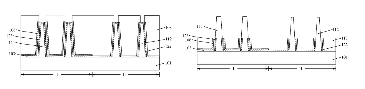
[0015]As shown in FIG. 11, at the beginning of fabrication process, a substrate with certain structures is provided (S101). FIG. 1 illustrates a corresponding semiconductor structure.

[0016]As shown in FIG. 1, a substrate 101 is provided. The substrate 101 may include a first region I and a second region II. A plurality of first fins 111 may be formed on the surface of the substrate 101 in the first region I; and a plurality of second fins 112 may be formed on the surface of the substrate 101 in the sec...


PUM


Abstract

The present disclosure provides fin field-effect transistors and fabrication methods thereof. An exemplary fabrication process includes providing a substrate having a first region and a second region; forming first fins in the first region and second fins in the second region; forming a liner oxide layer on side surfaces of the first fins, the second fins and a surface of the substrate; forming an insulating barrier layer on the liner oxide layer in the first region; forming a precursor material layer on the insulating barrier layer in the first region and on the liner oxide layer in the second region; performing a curing annealing process to convert the precursor material into an insulation layer; and removing a top portion of the insulation layer to form an isolating layer and removing portions of the liner oxide layer, the insulating barrier layer, the first oxide layer and the second oxide layer.

Description

CROSS-REFERENCES TO RELATED APPLICATIONS[0001]This application claims the priority of Chinese patent application No. 201610008863.2, filed on Jan. 7, 2016, the entirety of which is incorporated herein by reference.FIELD OF THE INVENTION[0002]The present invention generally relates to the field of semiconductor manufacturing technology and, more particularly, relates to fin field-effect transistors (FinFETs) and fabrication processes thereof.BACKGROUND[0003]With the rapid development of semiconductor manufacturing technology, the technical node of the semiconductor technology has been continuously shrunk by following the Moore's Law. To adapt to the reduced technical node, the channel length of the MOSFETs has to be continually reduced. Reducing the channel length of the MOSFETs is able to increase the device density of the integrate circuits (ICs); and increase the switching speed of the MOSFETs, etc.[0004]However, with the continuously shrinking the channel length, the distance bet...

Claims


Application Information

Patent Timeline
Patent Type & Authority Patents(United States)
IPC IPC(8): H01L21/311H01L27/088H01L21/3105H01L29/78H01L29/06H01L21/8234H01L21/324H01L29/66
CPCH01L29/66795H01L21/31053H01L21/31111H01L21/31144H01L29/785H01L21/823431H01L27/0886H01L29/0649H01L21/324
Inventor MAO, GANG
Owner SEMICON MFG INT (SHANGHAI) CORP
Why Eureka
Try Eureka