Semiconductor device

a semiconductor and semiconductor technology, applied in the field of semiconductor devices, can solve the problems of increasing the difficulty of manufacturing, memory cell formation, and improving the degree of integration of two-dimensional nonvolatile memory devices, and achieve the effect of improving stability and high yield manufacturing methods

Active Publication Date: 2018-11-13
SK HYNIX INC
View PDF8 Cites 1 Cited by
  • Summary
  • Abstract
  • Description
  • Claims
  • Application Information

AI Technical Summary

Benefits of technology

[0007]Embodiments of the present invention provide a three dimensional semiconductor device having an enhanced stable structure, and a high yield manufacturing method thereof.

Problems solved by technology

Recently, as further improvements in the degree of integration of two-dimensional nonvolatile memory devices in which memory cells are formed in a single layer over a silicon substrate have become very difficult, there has been proposed a three-dimensional nonvolatile memory device in which memory cells are vertically stacked on a silicon substrate.
However, as the height of the stack structure increases, the stress applied to the stack structure also increases.
Therefore, performance of three dimensional memory devices may suffer as the height of the stack structure increases.

Method used


Image

  • Semiconductor device
  • Semiconductor device
  • Semiconductor device

Examples


Embodiment Construction

[0021]Example embodiments of the present disclosure will be described with reference to the accompanying drawings. The example embodiments of the present disclosure may, however, be embodied in many different forms and should not be construed as limited to the example embodiments set forth herein. Rather, the example embodiments are provided so that disclosure of the present disclosure will be thorough and complete, and will fully convey the scope of the present disclosure to those skilled in the art. The features of example embodiments of the present disclosure may be employed in various and numerous embodiments without departing from the scope of the present disclosure. In the drawings, the size and relative sizes of layers and areas may be exaggerated for clarity. The drawings are not to scale. Like reference numerals refer to like elements throughout.

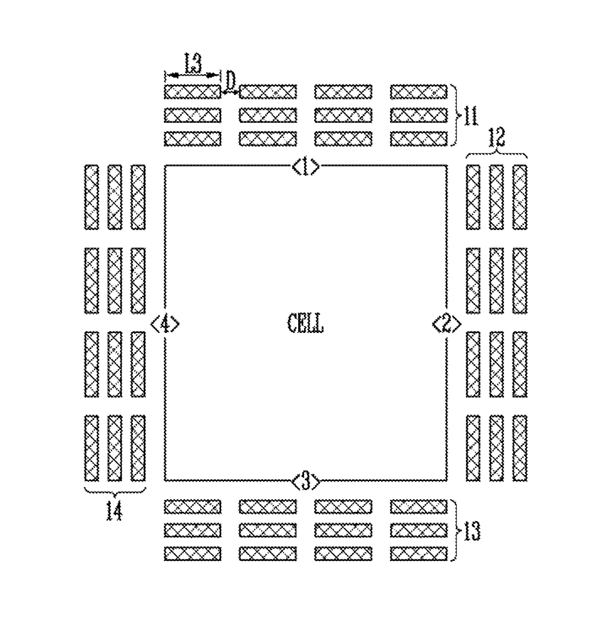
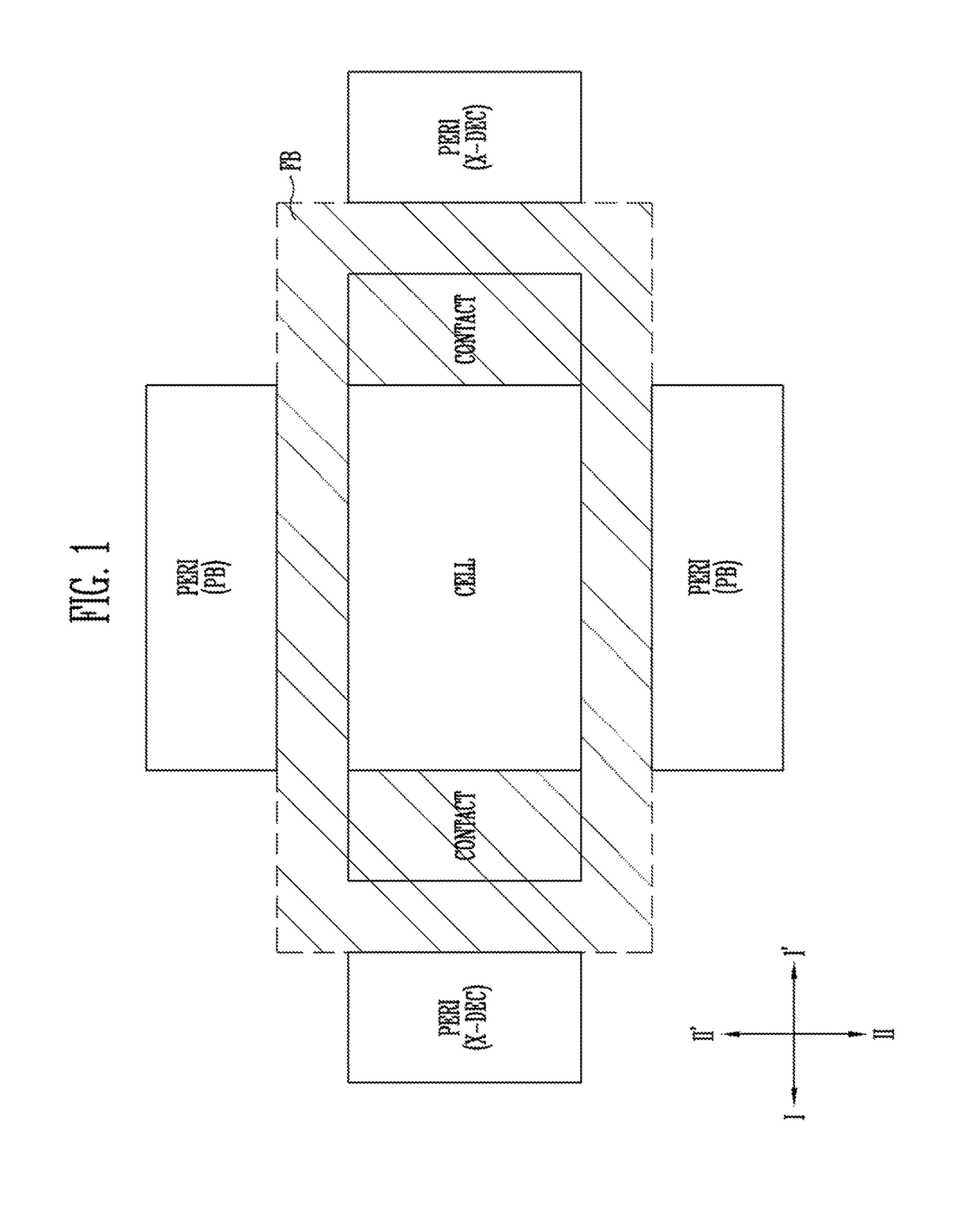
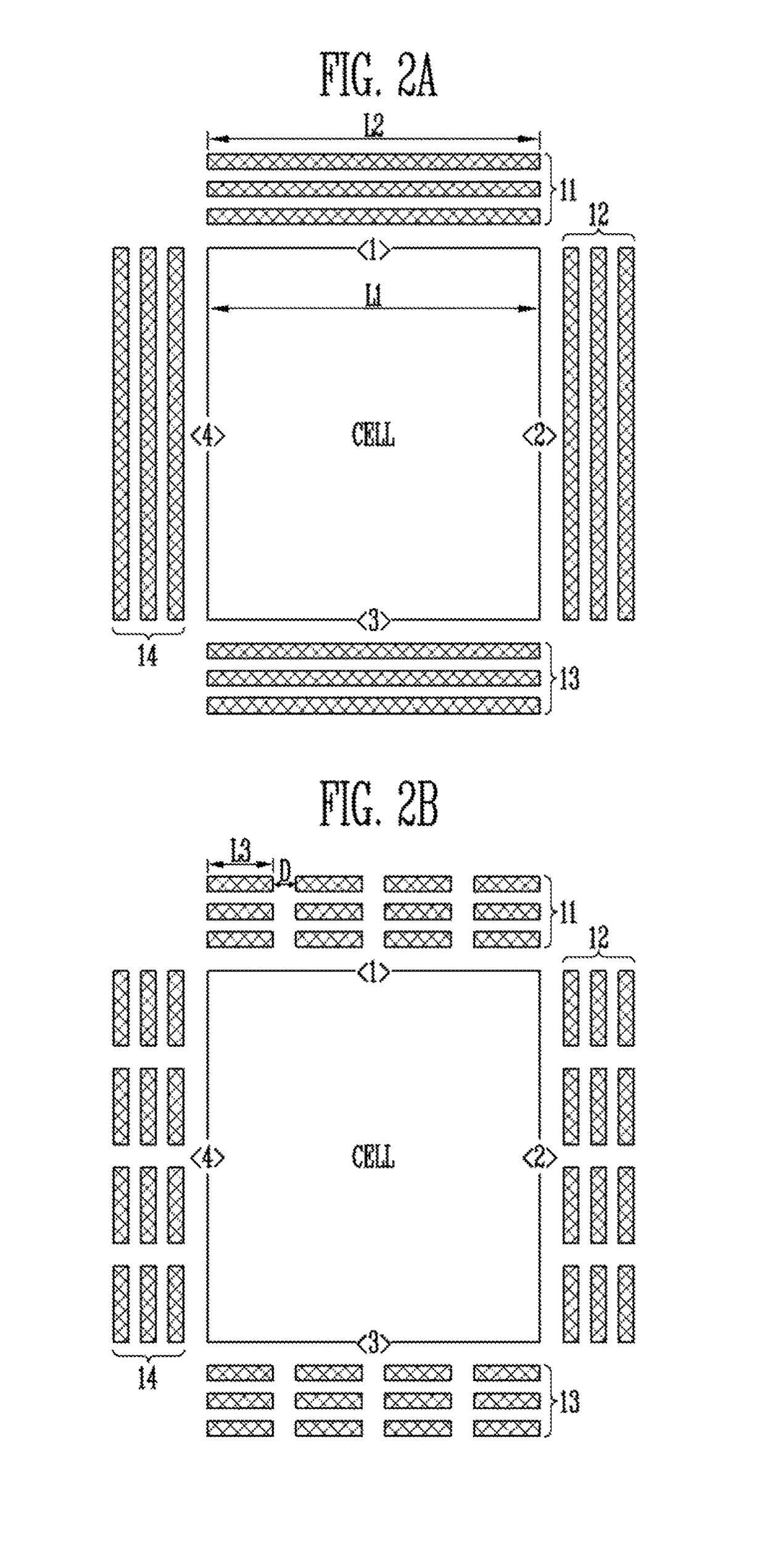
[0022]FIG. 1 is a layout Illustrating a structure of a semiconductor device, according to an embodiment of the present disclosure....


PUM


Abstract

A semiconductor device includes a substrate including a cell region and a peripheral region adjacent to the cell region, a cell stack structure located in the cell region, the cell stack structure including vertical memory strings, a circuit located in the peripheral region, the circuit driving the vertical memory strings, and an interlayer insulating layer formed on the substrate to cover the cell stack structure and the circuit, and including air gaps located between the cell region and the peripheral region.

Description

CROSS-REFERENCE TO RELATED APPLICATION[0001]The present application claims priority under 35 U.S.C 119(a) to Korean patent application number 10-2016-0012484 filed on Feb. 1, 2016, in the Korean Intellectual Property Office, the entire disclosure of which is incorporated herein in its entirety by reference.BACKGROUND[0002]1. Field[0003]An aspect of the present disclosure relates to an electronic device and, more particularly, to a semiconductor device having a three-dimensional structure and a manufacturing method thereof.[0004]2. Description of the Related Art[0005]Nonvolatile memory devices are memory devices which retain stored data even when a power supply to the device is cut off. Recently, as further improvements in the degree of integration of two-dimensional nonvolatile memory devices in which memory cells are formed in a single layer over a silicon substrate have become very difficult, there has been proposed a three-dimensional nonvolatile memory device in which memory cel...

Claims


Application Information

Patent Timeline
Patent Type & Authority Patents(United States)
IPC IPC(8): H01L27/115H01L27/11575H01L27/11524H01L27/11582H01L27/11526H01L27/11556H01L27/11548H01L27/1157H01L27/11573
CPCH01L27/11575H01L27/1157H01L27/11524H01L27/11582H01L27/11548H01L27/11556H01L27/11573H01L27/11526H10B43/35H10B43/10H10B43/50H10B43/40H10B43/27H10B41/27H10B41/35H10B41/40H10B41/50
Inventor CHUNG, SUNG JAE
Owner SK HYNIX INC
Why Eureka
Try Eureka