Dicing-tape integrated film for backside of semiconductor and method of manufacturing semiconductor device

a technology of integrated film and backside, which is applied in the direction of semiconductor devices, semiconductor/solid-state device details, thin material handling, etc., can solve the problems of inability to perform pickup and increase peel strength between dicing tape and the film for the backside of flip-chip semiconductors, so as to improve the yield ratio of flip-chip semiconductor devices, the effect of suppressing the occurrence of poor peeling in step d

Inactive Publication Date: 2018-11-27
NITTO DENKO CORP
View PDF8 Cites 0 Cited by
  • Summary
  • Abstract
  • Description
  • Claims
  • Application Information

AI Technical Summary

Benefits of technology

[0009]According to the above-described configuration, the difference (γ2−γ1) is 10 mJ / m2 or more. Therefore, the material constituting the film for the backside of a flip-chip semiconductor and the material constituting the pressure-sensitive adhesive layer differ in polarity. Because of that, the material constituting one of the layers hardly transfers into the other layer. Therefore, even when the film is heated, the increase of the peel strength between the dicing tape and the film for the backside of a flip-chip semiconductor can be suppressed.
[0011]In the above-described configuration, the pressure-sensitive adhesive layer preferably has a silicone pressure-sensitive adhesive layer at the interface with the film for the backside of a flip-chip semiconductor. The difference (γ2−γ1) can be easily made large when the pressure-sensitive adhesive layer has a silicone pressure-sensitive adhesive layer containing a silicone pressure-sensitive adhesive at the interface with the film for the backside of a flip-chip semiconductor.
[0012]In the above-described configuration, the pressure-sensitive adhesive layer preferably consists of a single layer of the silicone pressure-sensitive adhesive layer containing a silicone pressure-sensitive adhesive. The difference (γ2−γ1) can be easily made large when the pressure-sensitive adhesive layer consists of a single layer of the silicone pressure-sensitive adhesive layer containing a silicone pressure-sensitive adhesive.
[0019]According to the above-described configuration, because the film for the backside of a flip-chip semiconductor is used, the increase of the peel strength between the dicing tape and the film for the backside of a flip-chip semiconductor is suppressed even when the dicing-tape integrated film for the backside of a semiconductor is heated in the step A, etc. for example. Therefore, occurrence of poor peeling in the step D is suppressed. As a result, the yield ratio of the flip-chip semiconductor device can be improved.

Problems solved by technology

However, in the dicing-tape integrated film for the backside of a semiconductor, there is a problem that the peel strength between the dicing tape and the film for the backside of a flip-chip semiconductor increases due to heating when a wafer is pasted onto the film for the backside of a flip-chip semiconductor, and pickup cannot be performed.

Method used


Image

  • Dicing-tape integrated film for backside of semiconductor and method of manufacturing semiconductor device

Examples


example 1

[0150]

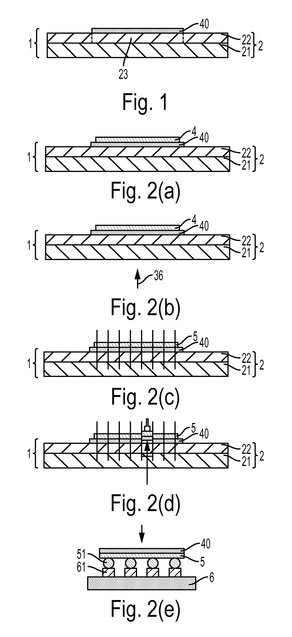
[0151]To 100 parts of an acrylic ester based polymer (Paracron W-197CM, manufactured by Negami Chemical Industrial Co., Ltd.) having ethylacrylate as a main component, 113 parts of an epoxy resin (Epicoat 1004, manufactured by Japan Epoxy Resins Co., Ltd.), 121 parts of a phenol resin (MEH-7851H, manufactured by Meiwa Plastic Industries, Ltd.), 246 parts of spherical silica (SO-25R, manufactured by ADMATECHS Co., Ltd.), and 5 parts of dye (OIL BLACK SOM-L-0543, manufactured by Orient Chemical Industries Co., Ltd.) were dissolved in methyethylketone to prepare an adhesive composition solution having a concentration of solid content of 23.6% by weight.

[0152]This adhesive composition solution was applied onto a release-treated film consisting of a silicon release-treated polyethyleneterephthalate film having a thickness of 50 μm as a release liner, and dried at 130° C. for 2 minutes to form a film A for the backside of a semiconductor having a thickness of 20 μm.

[0153]“OIL BLACK ...

example 2

[0158]The dicing-tape integrated film for the backside of a semiconductor according to Example 2 was produced in the same way as Example 1 except that TRM-3650S manufactured by NITTO DENKO CORPORATION was used as a dicing tape. TRM-3650S has a configuration in which a polyimide base material and a single silicone pressure-sensitive adhesive layer are laminated. TRM-3650S is used to be pasted onto the backside of a lead frame for masking to prevent resin leaking when the lead frame is sealed with a resin, and it is not a tape for dicing as a product.


PUM


Abstract

The present invention is to provide a dicing-tape integrated film for the backside of a semiconductor that is capable of suppressing the increase of the peel strength between the dicing tape and the film for the backside of a flip-chip semiconductor due to heating. The dicing-tape integrated film for the backside of a semiconductor has a dicing tape having a substrate and a pressure-sensitive adhesive layer formed on the substrate and a film for the backside of a flip-chip semiconductor formed on the pressure-sensitive adhesive layer of the dicing tape, in which the difference (γ2−γ1) of the surface free energy γ2 and the surface free energy γ1 is 10 mJ / m2 or more, where γ1 represents the surface free energy of the pressure-sensitive adhesive layer and γ2 represents the surface free energy of the film for the backside of a flip-chip semiconductor.

Description

BACKGROUND OF THE INVENTIONField of the Invention[0001]The present invention relates to a dicing-tape integrated film for the backside of a semiconductor and a method of manufacturing a semiconductor device.Description of the Related Art[0002]In recent years, thinning and downsizing of a semiconductor device and its packaging have been further required. Because of that, a flip-chip semiconductor device, in which a semiconductor element such as a semiconductor chip is flip-chip bonded on a substrate, has been widely used as a semiconductor device and its packaging. In the flip-chip bonding, a circuit surface of a semiconductor chip is fixed to an electrode forming surface of the substrate in a way that the circuit surface is facing to the electrode forming surface. In such semiconductor device, etc., the backside of the semiconductor chip may be protected by a film for the backside of a flip-chip semiconductor to prevent the semiconductor chip from damage, etc.[0003]Conventionally, t...

Claims


Application Information

Patent Timeline
Patent Type & Authority Patents(United States)
IPC IPC(8): H01L23/40H01L23/52H01L29/40H01L23/544H01L23/00H01L21/683
CPCH01L21/6836H01L23/544H01L24/83H01L24/84Y10T428/14H01L2924/15311H01L2224/92125H01L2224/83862H01L2224/83104H01L2224/83022H01L2224/83007H01L2224/81911H01L2224/81815H01L2224/81191H01L2224/81007H01L2224/73204H01L2224/32225H01L2224/2919H01L2224/16227H01L2224/13147H01L2224/13144H01L2224/13111H01L2224/131H01L2223/54486H01L2223/54433H01L2221/68377H01L2221/68327H01L24/92H01L24/73H01L24/32H01L24/13H01L24/16H01L24/29H01L2924/014H01L2924/00014H01L2924/01082H01L2924/01047H01L2924/01029H01L2924/0103H01L2924/01083H01L2924/0665H01L2924/066H01L24/81H01L2924/3512H01L2224/16225H01L2924/00
Inventor TAKAMOTO, NAOHIDEHANAZONO, HIROYUKIFUKUI, AKIHIRO
Owner NITTO DENKO CORP
Why Eureka
Try Eureka