Silicon carbide single crystal, silicon carbide single crystal wafer, silicon carbide single crystal epitaxial wafer, and electronic device

a technology of silicon carbide and single crystal, applied in the direction of crystal growth process, polycrystalline material growth, chemically reactive gas, etc., can solve the problem of significant deterioration of device characteristics, and achieve the effect of large distortion, large distortion, and improved device characteristics

Active Publication Date: 2019-01-15
DENSO CORP
View PDF10 Cites 0 Cited by
  • Summary
  • Abstract
  • Description
  • Claims
  • Application Information

AI Technical Summary

Benefits of technology

[0006]An object of the present disclosure is to provide a high-quality SiC single crystal, SiC single crystal wafer, and SiC single crystal epitaxial wafer that can improve device characteristics. Another object of the present disclosure is to provide an electronic device having improved device characteristics.
[0008]Device characteristics can be improved in such a manner that an electronic device includes a silicon carbide single crystal having a low density of threading dislocations with large distortion due to a large angle made between an orientation of a Burgers vector and an orientation of a dislocation line. Accordingly, a high-quality silicon carbide single crystal can be provided.
[0011]Device characteristics can be improved in such a manner that an electronic device is manufactured using a silicon carbide single crystal wafer having a low density of threading dislocations with large distortion. Accordingly, a high-quality silicon carbide single crystal wafer can be provided.
[0013]Device characteristics can be improved in such a manner that an electronic device is manufactured using a silicon carbide single crystal epitaxial wafer having a low density of threading dislocations with large distortion. Accordingly, a high-quality silicon carbide single crystal epitaxial wafer can be provided.
[0016]Since the electronic device includes the silicon carbide single crystal substrate or each of the silicon carbide single crystal substrate and the epitaxial growth layer having a low density of threading dislocations with large distortion, the device characteristics can be improved, as compared to a case of a high density of threading dislocations with large distortion.

Problems solved by technology

The present inventors have found that a large number of dislocations with such a large angle existing in the SiC single crystal would lead to significant deterioration of device characteristics.

Method used


Image

  • Silicon carbide single crystal, silicon carbide single crystal wafer, silicon carbide single crystal epitaxial wafer, and electronic device
  • Silicon carbide single crystal, silicon carbide single crystal wafer, silicon carbide single crystal epitaxial wafer, and electronic device
  • Silicon carbide single crystal, silicon carbide single crystal wafer, silicon carbide single crystal epitaxial wafer, and electronic device

Examples


first embodiment

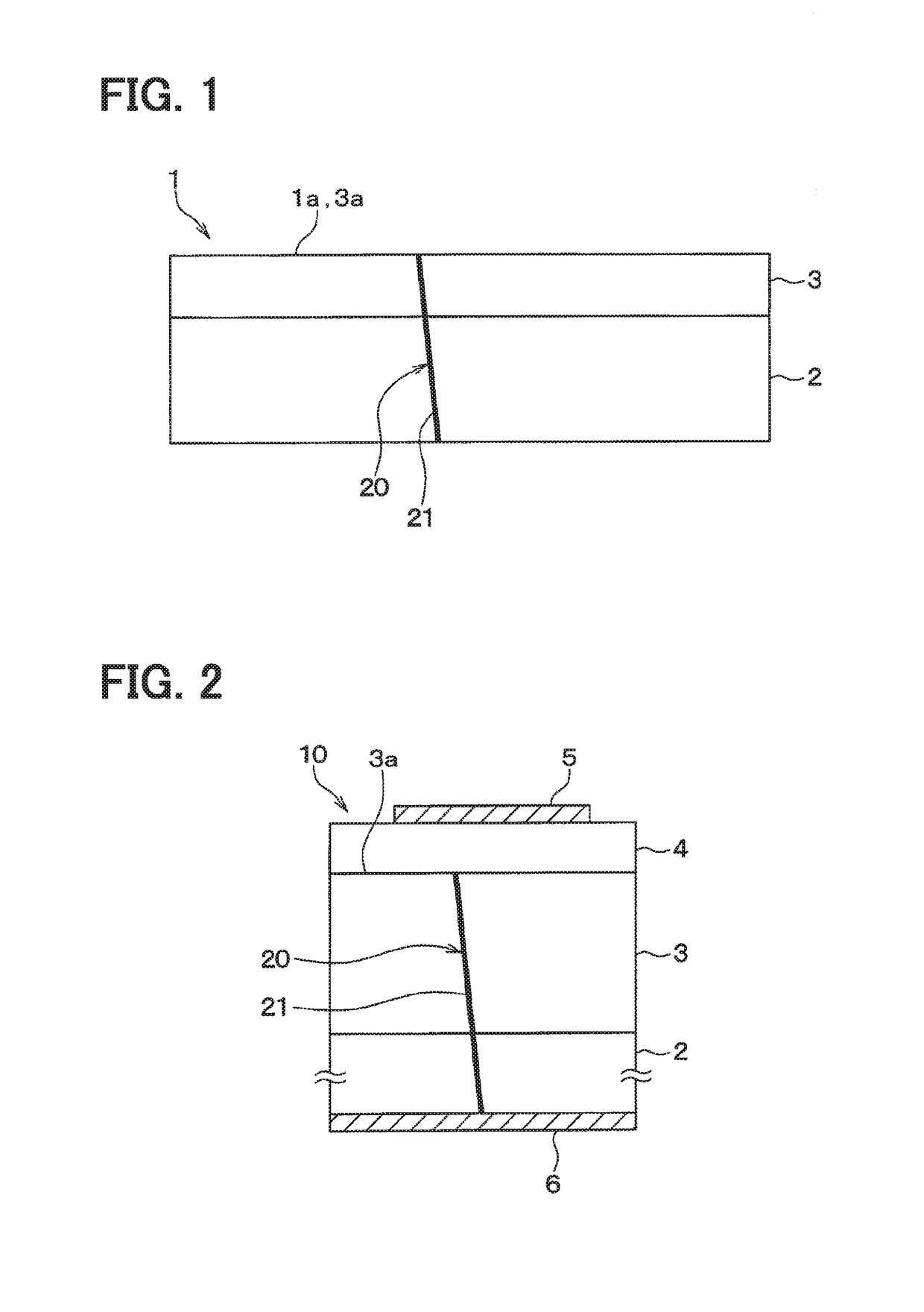
[0024](First Embodiment)

[0025]The present embodiment describes a SiC single crystal epitaxial wafer and a MOS capacitor manufactured using the SiC single crystal epitaxial wafer.

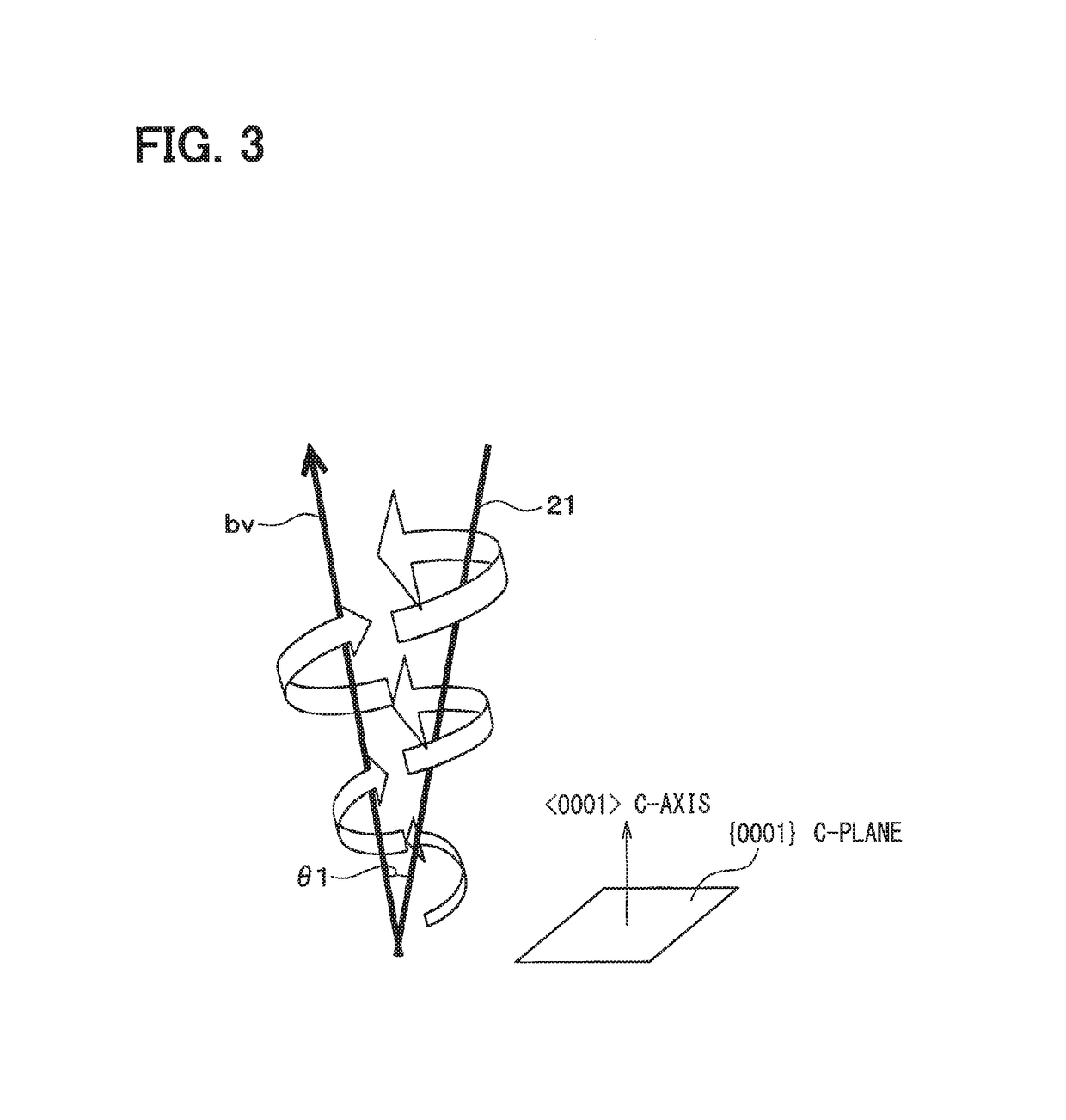
[0026]As illustrated in FIG. 1, a SiC single crystal epitaxial wafer 1 includes a SiC single crystal substrate 2, and a SiC epitaxial growth layer 3 formed by epitaxial growth on a surface of the SiC single crystal substrate 2. Hereinafter, the SiC single crystal epitaxial wafer 1 may also be referred to as a wafer 1, the SiC single crystal substrate 2 may also be referred to as a single crystal substrate 2, and the SiC epitaxial growth layer 3 may also be referred to as an epilayer 3. The SiC single crystal that forms the single crystal substrate 2 and the epilayer 3 has a polymorphism of 4H. An off-angle on a surface 1a of the wafer 1 (i.e., a surface 3a of the epilayer 3) is about 4° in a direction with respect to a {0001} plane. The epilayer 3 has a N-type conductivity. The SiC single crystal may have a...


PUM

PropertyMeasurementUnit
off-angleaaaaaaaaaa
off-angleaaaaaaaaaa
diameteraaaaaaaaaa

Abstract

A silicon carbide single crystal includes: threading dislocations each of which having a dislocation line extending through a C-plane, and a Burgers vector including at least a component in a C-axis direction. In addition, a density of the threading dislocations having angles, each of which is formed by an orientation of the Burgers vector and an orientation of the dislocation line, larger than 0° and within 40° is set to 300 dislocations / cm2 or less. Furthermore, a density of the threading dislocations having the angles larger than 40° is set to 30 dislocations / cm2 or less.

Description

CROSS REFERENCE TO RELATED APPLICATIONS[0001]This application is a U.S. national phase of International Application No. PCT / JP2016 / 074724 filed on Aug. 25, 2016 and is based on Japanese Patent Application No. 2015-170814 filed on Aug. 31, 2015, the disclosures of which are incorporated herein by reference.TECHNICAL FIELD[0002]The present disclosure relates to a silicon carbide (hereinafter referred to as SiC) single crystal, a SiC single crystal wafer, a SiC single crystal epitaxial wafer, and an electronic device.BACKGROUND ART[0003]Patent Literature 1 describes a high-quality SiC single crystal. The SiC single crystal in Patent Literature 1 is required to classify spiral dislocations into dislocations with large distortion and dislocations with small distortion based only on a Burgers vector, and to have a low density of the dislocations with large distortion.PRIOR ART LITERATURESPatent Literature[0004]Patent Literature 1: JP 2014-159351 ASUMMARY OF INVENTION[0005]According to an ...

Claims


Application Information

Patent Timeline
Patent Type & Authority Patents(United States)
IPC IPC(8): C23C16/32C30B29/36H01L29/66H01L29/94H01L29/04H01L29/32H01L21/02H01L29/16C30B25/18
CPCH01L29/1608C30B29/36H01L21/02378H01L21/02433H01L21/02529H01L21/02634H01L29/045H01L29/32H01L29/6606H01L29/94H01L21/02609C30B25/18H01L21/02293H01L21/0243H01L21/02598
Inventor OKAMOTO, TAKESHIKONDO, HIROYUKIKANEMURA, TAKASHIMIYAHARA, SHINICHIROEBIHARA, YASUHIROONDA, SHOICHITSUCHIDA, HIDEKAZUKAMATA, ISAHOTANUMA, RYOHEI
Owner DENSO CORP
Why Eureka
Try Eureka