Track-and-hold circuit with acquisition glitch suppression

a track and hold circuit and suppression technology, applied in information storage, electric analogue stores, static storage, etc., can solve the problems of input level compatibility problems, high energy consumption, and high energy consumption of acquisition glitches, and achieve the effect of mitigating the magnitude of differential acquisition glitches

Active Publication Date: 2019-01-29
HITTITE MICROWAVE LLC
View PDF10 Cites 1 Cited by
  • Summary
  • Abstract
  • Description
  • Claims
  • Application Information

AI Technical Summary

Benefits of technology

[0004]This invention features a switched track-and-hold circuit with acquisition glitch suppression including a track-and-hold circuit. The track-and-hold circuit includes a switching circuit and a plurality of storage devices. The switching circuit is responsive to an input signal and configured to apply a representation of the input signal to the storage devices in a track mode and block a signal path between the input signal and the storage device in a hold mode such that a transition from the track mode to a hold mode causes the storage devices to store a time sample of the input signal. An acquisition glitch suppression circuit includes a replica amplifier coupled to the switching circuit configured to sense a differential voltage across the storage devices. A switched clamping circuit is configured to clamp inputs of the switching circuit to the sensed differential voltage in the hold mode such that the initial condition of switching transistors of the switching circuit are approximately identical prior to a hold to track transition to mitigate differential acquisition glitch magnitude.
[0006]This invention also features a method of mitigating an acquisition glitch for a switched track-and-hold circuit. The method includes the steps of: applying a representation of an input signal to a plurality of storage devices of a track-and-hold circuit in a track mode, blocking a signal path between the input signal and the plurality of storage devices in a hold mode such that a transition from the track mode to the hold mode causes the storage devices to store a time sample of the input signal, and sensing the differential voltage across the storage devices, and clamping the inputs of the switching circuit to the sensed differential voltage in the hold mode such that the initial condition of voltages across of the switching circuit are approximately identical prior to a hold-to-track transition to mitigate the differential acquisition glitch magnitude.
[0007]In another embodiment, the method may further include the step of clamping the inputs of the switching circuit to the sensed differential voltage in the hold mode such that the initial condition of switching transistors of the switching may be approximately identical prior to a hold-to-track transition to mitigate acquisition glitch. The method may include the step of providing a plurality of switched emitter followers. The method may include the step of setting the base voltages of each of emitter followers to a predetermined value to create identical conditions on each base-emitter capacitance of each emitter follower.

Problems solved by technology

As a result, the T / H may often exhibit glitches in its output waveform, often referred to as acquisition glitches.
The acquisition glitch is typically impulsive and has very high energy and very short time duration.
The acquisition glitch may cause input level compatibility problems in ADCs.
The ringing / settling time associated with the response of the ADCs to the glitch can slow down the permissible sample rate and degrade conversion accuracy.

Method used


Image

  • Track-and-hold circuit with acquisition glitch suppression
  • Track-and-hold circuit with acquisition glitch suppression
  • Track-and-hold circuit with acquisition glitch suppression

Examples


Embodiment Construction

[0018]Aside from the preferred embodiment or embodiments disclosed below, this invention is capable of other embodiments and of being practiced or being carried out in various ways. Thus, it is to be understood that the invention is not limited in its application to the details of construction and the arrangements of components set forth in the following description or illustrated in the drawings. If only one embodiment is described herein, the claims hereof are not to be limited to that embodiment. Moreover, the claims hereof are not to be read restrictively unless there is clear and convincing evidence manifesting a certain exclusion, restriction, or disclaimer.

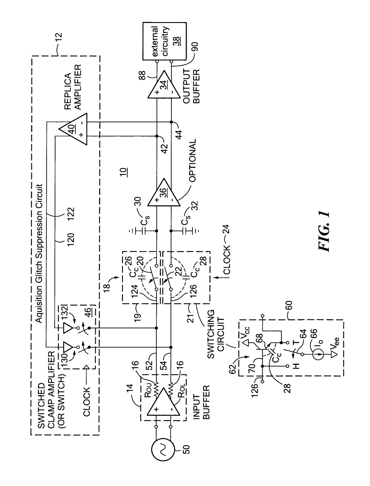
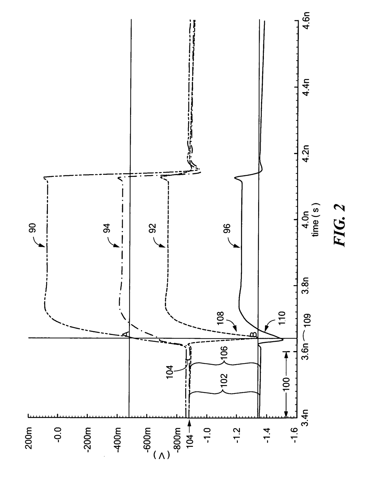
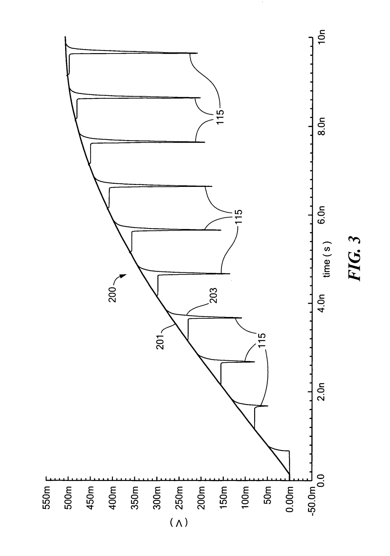
[0019]As discussed in the Background section above, conventional T / H circuits often exhibit acquisition glitches in their output waveforms. For example, one conventional T / H circuit utilizes a switched emitter-follower (SEF) to provide high speed signal sampling and signal conditioning with a wide bandwidth that can extend ...


PUM


Abstract

The track-and-hold circuit includes a switching circuit and a plurality of storage devices. The switching circuit responsive to an input signal applies a representation of the input signal to the storage devices in a track mode and blocks a signal path between the input signal and the storage device in a hold mode such that a transition from the track mode to a hold mode causes the storage devices to store a time sample of the input signal. An acquisition glitch suppression circuit includes a replica amplifier coupled to the switching circuit that senses a differential voltage across the storage devices. A switched clamping circuit clamps inputs of the switching circuit to the sensed differential voltage in the hold mode such that the initial condition of switching transistors of the switching circuit are approximately identical prior to a hold-to-track transition to mitigate differential acquisition glitch.

Description

FIELD OF THE INVENTION[0001]This invention relates to a track-and-hold circuit with acquisition glitch suppression.BACKGROUND OF THE INVENTION[0002]A track-and-hold circuit (T / H) may be used to sample and condition analog signals. A T / H is often used at the front end of analog-to-digital converters (ADCs) to sample a signal and then hold the signal sample constant-such that conversion circuitry of the ADC has time to convert and process the sample. The T / H function typically involves high speed switching of analog signals. As a result, the T / H may often exhibit glitches in its output waveform, often referred to as acquisition glitches. The acquisition glitch, which occurs after the hold-to-track transition when the device is tracking and acquiring the signal, tends to be the dominant glitch or perturbation in the output waveform of a switched T / H, such as a switched emitter follower (SEF) T / H, a diode bridge switched T / H, or similar type switched T / H. The acquisition glitch is typic...

Claims


Application Information

Patent Timeline
Patent Type & Authority Patents(United States)
IPC IPC(8): G11C27/02
CPCG11C27/02G11C27/028G11C27/024G11C27/026
Inventor HOSKINS, MICHAEL J.
Owner HITTITE MICROWAVE LLC
Why Eureka
Try Eureka