

Semiconductor device
a semiconductor and device technology, applied in the direction of semiconductor devices, semiconductor/solid-state device details, electrical apparatus, etc., can solve the problems of excessive fault current, electric arcing inside the device, and the device loses its blocking capability, so as to reduce the non-rupture capability of the housing, the case-non-rupture current is higher, and the non-rupture capability is limited.
- Summary
- Abstract
- Description
- Claims
- Application Information
AI Technical Summary
Benefits of technology
Problems solved by technology
Method used
Image

Examples
Embodiment Construction
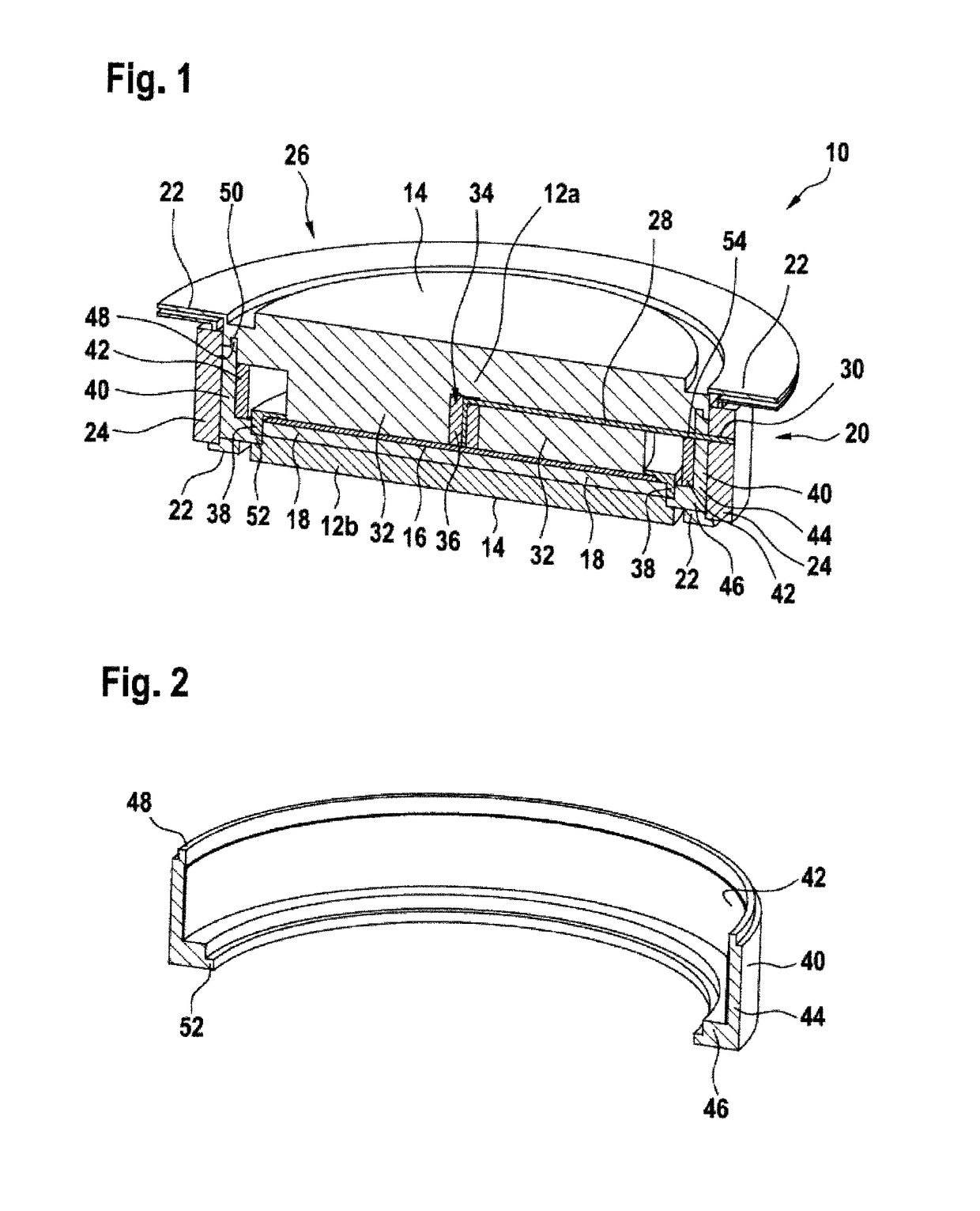
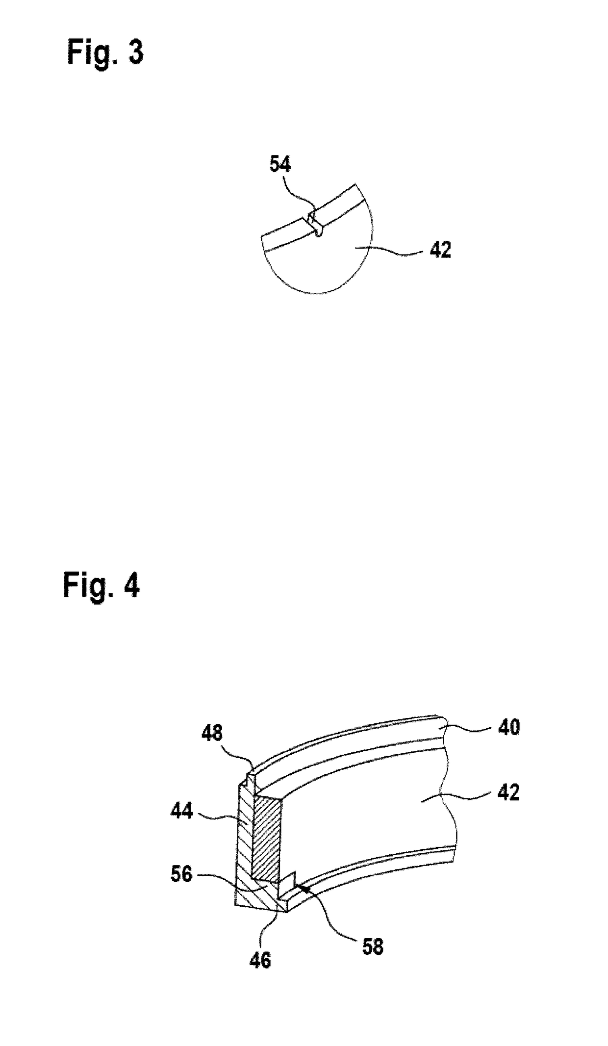
[0010]Sometimes, due to the arc, pressure may develop inside the housing due to ablation of a polymer material, which also may limit the non-rupture capabilities of the housing of the semiconductor device.
[0011]It is an objective of the invention to enhance non-rupture capabilities of a semiconductor device.
[0012]This objective is achieved by the subject-matter of the independent claim. Further exemplary embodiments are evident from the dependent claims and the following description.
[0013]The invention relates to a semiconductor module or semiconductor device, which may be a power semiconductor module / device adapted for switching currents of more than 10 A and / or 1.000 V.
[0014]According to an embodiment of the invention, the semiconductor device comprises two electrodes with opposite faces, a semiconductor wafer sandwiched between the two electrodes, an outer insulating ring attached to the two electrodes and surrounding the semiconductor wafer, a middle insulating ring inside the o...
PUM
 Abstract
Description
Claims
Application Information