Check patentability & draft patents in minutes with Patsnap Eureka AI!

Photodiode array

a photodiode array and array technology, applied in the field of photodiode arrays, can solve the problems of inability to count photons and shorten the interval between output pulse signals, and achieve the effect of reducing recovery time, reducing recovery time and reducing recovery tim

Active Publication Date: 2019-03-05
HAMAMATSU PHOTONICS KK
View PDF24 Cites 3 Cited by
  • Summary
  • Abstract
  • Description
  • Claims
  • Application Information

AI Technical Summary

Benefits of technology

The present invention is a photodiode array that has a second contact electrode positioned overlapping the first contact electrode. This arrangement reduces the space required for connecting the resistive layer and the first contact electrode. The first and second contact electrodes are at different height positions, and the resistive layer extends from the second contact electrode. This eliminates wiring in the light detecting sections, increasing the aperture ratio. Additionally, the invention shortens the recovery time of the photodiode, resulting in a high count rate.

Problems solved by technology

However, in the case where a plurality of photons are made incident to an APD at short time intervals, an interval between the output pulse signals is shortened, to be unable to perform pulse separation, which makes it incapable of photon counting.

Method used


Image

  • Photodiode array
  • Photodiode array
  • Photodiode array

Examples


Embodiment Construction

[0032]Hereinafter, a photodiode array according to an embodiment will be described. In addition, the same reference numerals are to be used for the same components, and overlapping descriptions will be omitted.

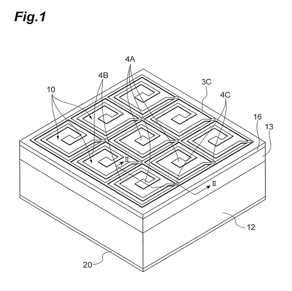
[0033]FIG. 1 is a perspective view of a photodiode array, and FIG. 2 is a longitudinal sectional view taken along arrows II to II of the photodiode array.

[0034]This photodiode array has a light receiving region on the surface side of a semiconductor substrate made of Si. The light receiving region includes a plurality of light detecting sections (light detection channels) 10, and these light detecting sections 10 are two-dimensionally arrayed in a matrix state. In addition, the light detecting sections 10 in three rows and in three columns are arrayed, and these compose the light receiving region. Meanwhile, the number of the light detecting sections 10 may be larger or smaller, and may be configured to be one-dimensionally arrayed.

[0035]A wiring pattern (top surface electrode...


PUM


Abstract

A light receiving region includes a plurality of light detecting sections 10. The light detecting sections 10 has a second contact electrode 4A. The second contact electrode 4A is arranged at a position overlapping a first contact electrode 3A, so as to contact the first contact electrode. Further, a resistive layer 4B is continued to the second contact electrode 4A.

Description

[0001]This is a continuation application of copending prior application Ser. No. 14 / 314,616, filed on Jun. 25, 2014, which is a continuation of prior application Ser. No. 13 / 655,907 filed on Oct. 19, 2012, which is issued as U.S. Pat. No. 8,791,538. The prior application Ser. Nos. 13 / 655,907 and 14 / 314,616 are incorporated by reference herein in their entireties.TECHNICAL FIELD[0002]An aspect of the present invention relates to a photodiode array.BACKGROUND[0003]A conventional photodiode array is described in, for example, the following Patent Document 1. A photodiode array such as an SiPM (Silicon Photo Multiplier) or a PPD (Pixelated Photon Detector) has a configuration in which APDs (avalanche photodiodes) are arrayed in a matrix state, and the plurality of APDs are connected in parallel, to read out a sum of APD outputs. When the APDs are operated in the Geiger mode, it is possible to detect feeble light (photons). That is, in the case where photons are made incident to an APD, ...

Claims


Application Information

Patent Timeline
Patent Type & Authority Patents(United States)
IPC IPC(8): H01L29/76H01L27/144H01L27/146H01L31/0224H01L31/107H01L49/02H01L31/02H10N97/00
CPCH01L27/14643H01L27/1443H01L27/1446H01L27/14605H01L27/14607H01L31/107H01L27/14636H01L28/24H01L31/02027H01L31/022416H01L31/022466H01L27/14609
Inventor YAMAMOTO, KOEINAGANO, TERUMASAYAMAMURA, KAZUHISASATO, KENICHITSUCHIYA, RYUTARO
Owner HAMAMATSU PHOTONICS KK
Features
  • R&D
  • Intellectual Property
  • Life Sciences
  • Materials
  • Tech Scout
  • Unparalleled Data Quality
  • Higher Quality Content
  • 60% Fewer Hallucinations
Learn More