Semiconductor device

a technology of a semiconductor and a gate, which is applied in the direction of semiconductor devices, basic electric elements, electrical appliances, etc., can solve the problems that the structure of fig. 11 cannot cope with and the problem of reducing the withstand voltage between the drain and the source cannot be solved, so as to reduce the withstand voltage of the gate, reduce the potential difference, and reduce the effect of resistan

Active Publication Date: 2019-04-09
DENSO CORP
View PDF19 Cites 0 Cited by
  • Summary
  • Abstract
  • Description
  • Claims
  • Application Information

AI Technical Summary

Benefits of technology

[0013]With the above arrangement, the on-resistance is reduced due to the presence of the n-type impurity high-concentration region, and reduction of the gate withstand voltage can be curbed by reducing a potential difference across the insulating film due to the presence of the n-type impurity low-concentration region. Further, since the n-type impurity low-concentration region is in contact with the p-type well region, the intensity of electric field in the vicinity of an interface between these regions is reduced, and avalanche breakdown is less likely or unlikely to occur, so that current can be prevented from flowing into the inside-of-well n-type region. It is also possible to cope with a problem of reduction of the withstand voltage between the drain and the source.

Problems solved by technology

However, the structure of FIG. 11 cannot cope with the problem of reduction of the withstand voltage between the drain and the source.
With the technology of JP 2012-064741A, the problem of reduction of the withstand voltage between the drain and the source cannot be coped with or solved.

Method used


Image

  • Semiconductor device
  • Semiconductor device
  • Semiconductor device

Examples


first embodiment

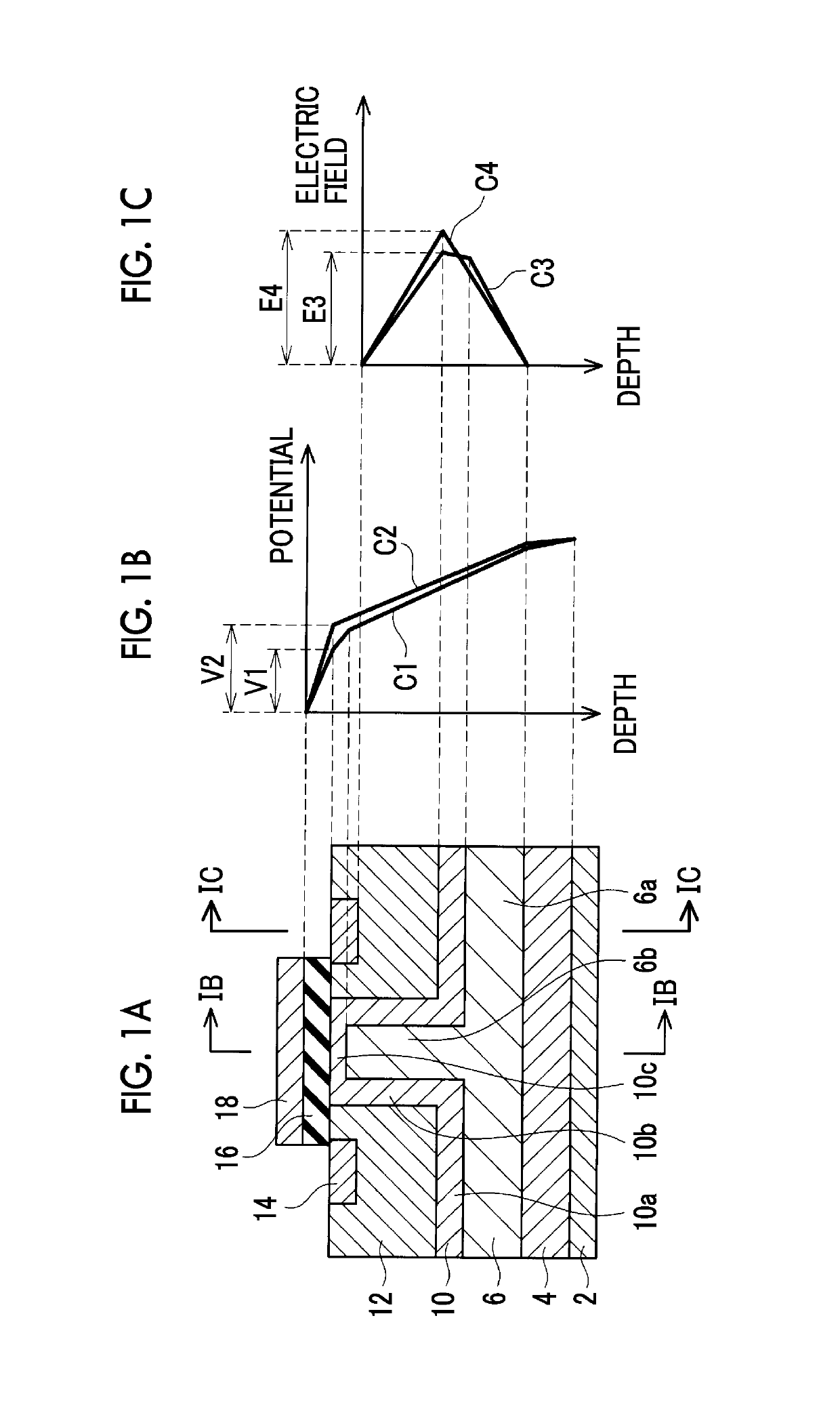
[0033]FIG. 1A shows a semiconductor device of a first embodiment in cross-section. In this embodiment, outside-of-well n-type regions 6, 10 provide an n-type drift region, and a p-type well region 12 provides a p-type body region, while an inside-of-well n-type region 14 provides an n-type source region.

[0034]In FIG. 1A, reference numeral 2 denotes a drain electrode formed on a rear surface of a semiconductor substrate. Reference numeral 4 denotes a drain region including a high concentration of n-type impurity, which is in ohmic contact with the drain electrode 2. As will be apparent from a production method that will be described later, the drain region 4 consists of a seed substrate with which epitaxial growth is started. The semiconductor device of FIG. 1A was produced by using the seed substrate having a suitable concentration of n-type impurity, as the drain region 4.

[0035]In FIG. 1A a pair of p-type body regions 12, 12 are illustrated. The number of the body regions is not pa...

second embodiment

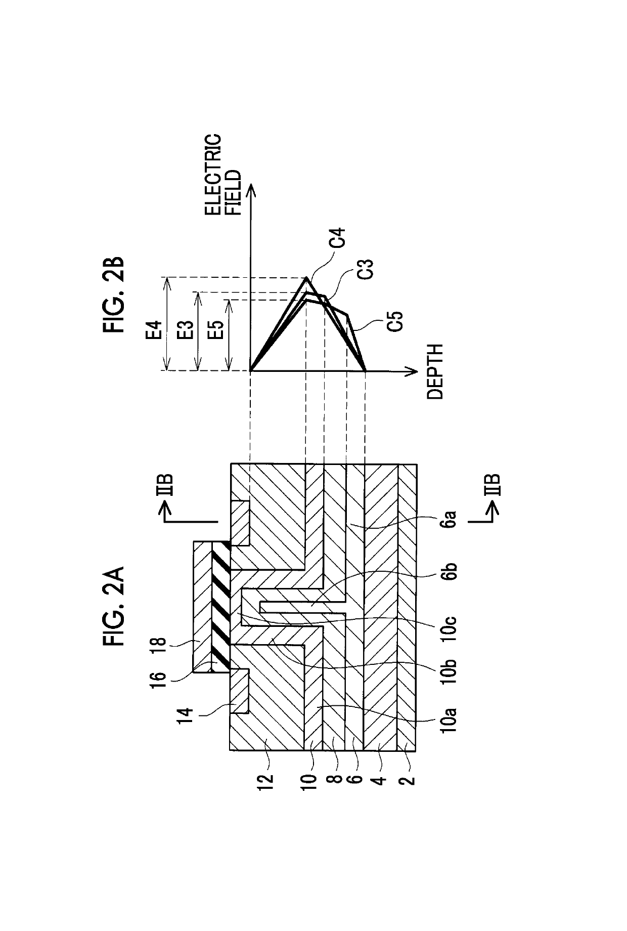
[0042]In a second embodiment, an n-type middle-concentration drift region 8 is formed between an n-type low-concentration drift region 10 and an n-type high-concentration drift region 6, as shown in FIG. 2A. In FIG. 2B, which corresponds to FIG. 1C, graphs C3, C4 are those as described above with reference to FIG. 1C. Graph C5 indicates the electric field intensity of the semiconductor device shown in FIG. 2A, and E5 indicates the maximum electric field intensity of the semiconductor device shown in FIG. 2A. Graph C5 of FIG. 2B shows the intensity of electric field generated at respective positions along line IIB-IIB in FIG. 2A. Apparently, E5 is smaller than E4, and E5 is smaller than E3. If the middle-concentration drift region 8 is added to between the low-concentration drift region 10 and the high-concentration drift region 6, the withstand voltage between the source and the drain is improved.

[0043]While a single sheet of middle-concentration drift region 8 is added to between t...


PUM


Abstract

A semiconductor device includes an outside-of-well n-type region, a p-type well region surrounded by the outside-of-well n-type region, an inside-of-well n-type region, and a gate electrode. The outside-of-well n-type region includes an impurity low-concentration region that is in contact with the p-type well region, and an impurity high-concentration region that is separated from the p-type well region by the impurity low-concentration region.

Description

INCORPORATION BY REFERENCE[0001]The disclosure of Japanese Patent Application No. 2016-199498 filed on Oct. 7, 2016 including the specification, drawings and abstract is incorporated herein by reference in its entirety.BACKGROUND[0002]1. Technical Field[0003]The disclosure relates to a semiconductor device.[0004]2. Description of Related Art[0005]As illustrated in FIG. 10 by way of example, a field effect transistor (FET) including an n-type drift region 6, p-type well regions 12, n-type source regions 14, insulating film 16, and a gate electrode 18 is known. The p-type well regions 12 are surrounded by the n-type drift region 6, and are exposed to a surface of a semiconductor substrate. The n-type source regions 14 are surrounded by the p-type well regions 12, and are exposed to the surface of the semiconductor substrate. The gate electrode 18 is opposed, via the insulating film 16, to a surface of each p-type well region 12 in a range in which the n-type drift region 6 and the n-t...

Claims


Application Information

Patent Timeline
Patent Type & Authority Patents(United States)
IPC IPC(8): H01L29/06H01L29/10H01L21/324H01L21/306H01L29/20H01L21/265H01L29/739H01L21/02H01L29/78
CPCH01L29/063H01L21/0254H01L21/02576H01L21/26546H01L21/3245H01L29/1095H01L29/2003H01L29/7395H01L21/30617H01L29/7802H01L29/0607H01L29/7393H01L29/78H01L29/66712H01L29/0878H01L29/0886H01L29/808H01L29/1058
Inventor KAWAKAMI, MASAHIROMORI, TOMOHIKOUEDA, HIROYUKI
Owner DENSO CORP
Why Eureka
Try Eureka