Semiconductor device and method for manufacturing the same

a semiconductor and metal-insulator technology, applied in the direction of semiconductor devices, electrical devices, transistors, etc., can solve the problems of reducing withstand voltage, unable to achieve sufficient reduced withstand voltage as the whole device, and sub>2 /sub>on the bottom of the trench does not contribute to reducing on-resistance, etc., to achieve improved withstand voltage, reduce on-resistance, and improve withstand voltage

Inactive Publication Date: 2011-03-01
FUJI ELECTRIC CO LTD
View PDF10 Cites 0 Cited by
  • Summary
  • Abstract
  • Description
  • Claims
  • Application Information

AI Technical Summary

Benefits of technology

[0031]According to the embodiments of the invention, the shape of the electric field distribution approaches from a triangular shape (see FIG. 49) to a rectangular shape (see FIG. 2) when the maximum electric field strength reaches the critical electric field strength in the off-state under the influence of polarized charges in the high-permittivity dielectric region under the gate electrode. The area of the electric field distribution increases accordingly, and this area corresponds to the withstand voltage, resulting in improved withstand voltage. Therefore, a higher withstand voltage is achieved even if the impurity concentration in the drift region is the same as the conventional value. That is, when the withstand voltage class is the same as the conventional value, on-resistance is reduced. Furthermore, although conventionally it has not been easy to fill the portion under the gate electrode, in the trench, with a high-permittivity dielectric having relative permittivity higher than that of a silicon nitride film under the gate electrode, according to the invention, the lower half of the trench is filled with a high-permittivity dielectric and the gate electrode is formed in the upper half of the same trench.

Problems solved by technology

However, in the semiconductor device disclosed in U.S. Patent Application Publication No. 2004 / 0166636, it is apparent from the document that the thick SiO2 on the bottom of the trench does not contribute to reduction in on-resistance.
Therefore, although extending the N-epitaxial layer (drift region) may reduce its concentration, it increases the proportion of the resistance of the N-epitaxial layer (drift region) relative to the total on-resistance, so that an increased number of gate electrodes by employing the trench gate structure unfortunately cannot achieve sufficient reduced on-resistance as the whole device.
When the numbers of carriers in the n-drain / drift region and the p-type impurity layer are not balanced, the depletion layer will not expand due to residual carriers in the off-state, resulting in reduced withstand voltage.
In the semiconductor device disclosed in WO 2004 / 102670, as the field formation region is an idle region where no on-current flows, provision of the field formation region increases the width of a unit element, disadvantageously resulting in lower integration level.
Furthermore, to fabricate this semiconductor device, it is necessary to form a trench for the gate electrode as well as a trench for the field formation region that is deeper than the gate electrode trench with these trenches tightly close to each other and separately fill these trenches, unfortunately resulting in very difficult fabrication.
However, according to a study conducted by the inventors, it has been found that the structure shown in FIG. 7 in WO 2004 / 102670 would hardly provide effects comparable to the simulation results.
Even if the depletion layer is forced to expand into the p-body, the depletion layer will reach the source region, resulting in punch through.
Conversely, there is created an undesired portion around the gate electrode where the electric field concentrates, disadvantageously resulting in reduced withstand voltage.
Furthermore, the extended p-body increases the length of the channel, disadvantageously resulting in increased on-resistance.
In the semiconductor device disclosed in JP-A-2003-204064, provision of the field plate disadvantageously prevents higher integration level.

Method used


Image

  • Semiconductor device and method for manufacturing the same
  • Semiconductor device and method for manufacturing the same
  • Semiconductor device and method for manufacturing the same

Examples


first embodiment

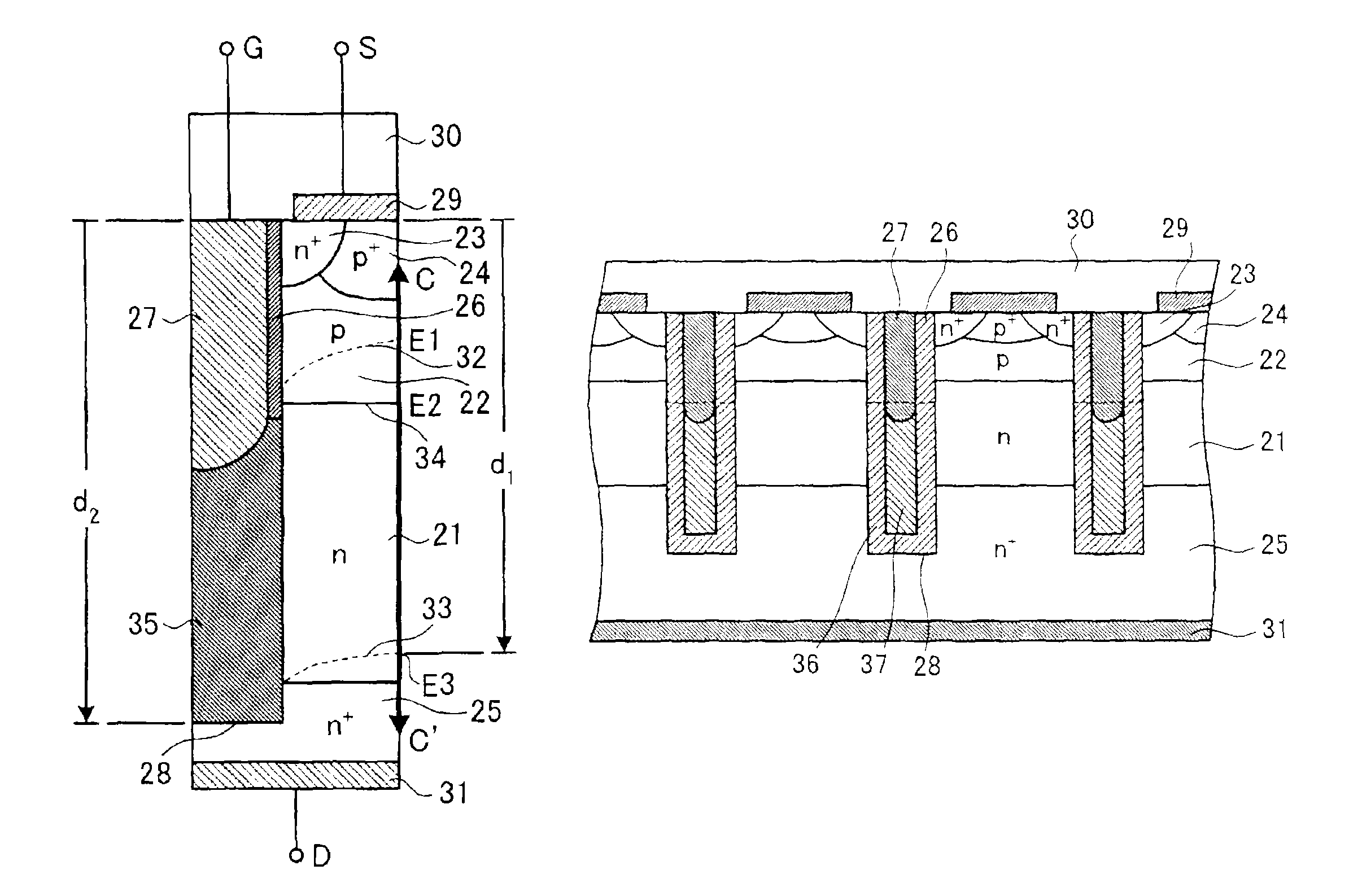
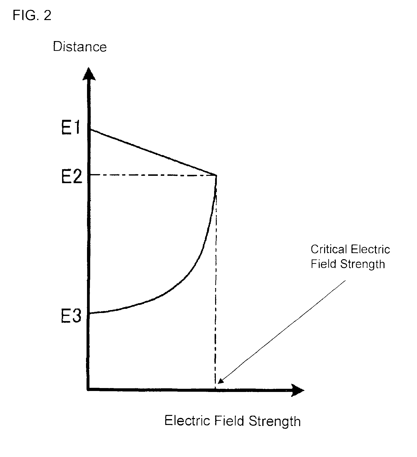
[0084]FIG. 1 is a cross-sectional view showing the configuration of the trench gate type MISFET according to a first embodiment of the invention. FIG. 1 shows a half cell including the main portion of the semiconductor device. The overall configuration of the actual semiconductor device has the half cell configurations shown in FIG. 1 in succession on both sides such that adjacent configurations are symmetric with respect to the edge line there between (the same thing applies to FIG. 14).

[0085]As shown in FIG. 1, in the vertical trench gate type n-channel MISFET according to the first embodiment, p-base region 22 is formed on a first principal surface side across n-drift region 21, while n+-drain region 25 is formed on a second principal surface side across n-drift region 21. N+-source region 23 and p+-contact region 24 are formed adjacent to each other on the surface layer of p-base region 22.

[0086]Trench 28, formed adjacent to n+-source region 23, extends from the first principal ...

second embodiment

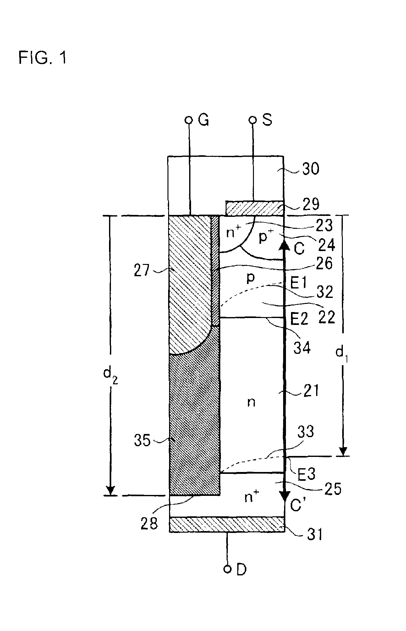
[0103]FIG. 14 is a cross-sectional view showing the configuration of a half cell of the trench gate type MISFET according to a second embodiment of the invention. As shown in FIG. 14, the MISFET according to the second embodiment differs from the first embodiment in that high-permittivity dielectric 35 buried under gate electrode 27 has a double-layer structure including high-permittivity dielectric 36 in an outer portion and high-permittivity dielectric 37 in an inner portion. As other structures are the same as those of the first embodiment, they have the same reference characters and description thereof will be omitted.

[0104]The relative permittivity of high-permittivity dielectrics 36 and 37 in the outer and inner portions is advantageously selected to be higher than that of a silicon oxide film (SiO2), preferably higher than that of a silicon nitride film (Si3N4). Examples of these high-permittivity dielectrics 36 and 37 include the various materials exemplified in the first em...

third embodiment

[0121]FIGS. 37 to 44 are cross-sectional views showing a method for manufacturing the trench gate type MISFET according to a third embodiment of the invention. Firstly, an n-semiconductor layer, which will be n-drift region 21, is epitaxially grown on n+-substrate, which will be n+-drain region 25. Subsequently, a p-type impurity, such as boron ions, is implanted into the surface of the epitaxially grown layer, followed by thermal diffusion to provide a p-semiconductor layer, which will be p-base region 22 (FIG. 37).

[0122]Thereafter, reactive ion etching is used to form trench 28 extending from the surface of the p-semiconductor layer into the n+-substrate (FIG. 38). Then, thermal oxidation is used to cover the inner surface of trench 28 with a silicon oxide film (SiO2) (FIG. 39). The silicon oxide film is high-permittivity dielectric 36 in the outer portion in the MISFET according to the second embodiment. By covering the inner surface of trench 28 with the silicon oxide film, the ...


PUM


Abstract

In a MIS-type semiconductor device having a trench gate structure, a withstand voltage is ensured without changing the thickness of a drift layer and on-resistance can be reduced without applying a high gate drive voltage. The lower half of a trench extending through a p-base region into an n-drift region is filled with a high-permittivity dielectric having a relative permittivity that is higher than that of a silicon oxide film, preferably a silicon nitride film, and an insulated gate structure including a gate insulator and a gate electrode is fabricated on the high-permittivity dielectric. The depth d2 of the deepest portion of the high-permittivity dielectric is designed to be deeper than the depth d1 of a depletion layer in the semiconductor region away from the high-permittivity dielectric.

Description

CROSS REFERENCE TO RELATED APPLICATIONS[0001]This application claims priority from Japanese application Serial No. 2007-021828, filed on Jan. 31, 2007.BACKGROUND OF THE INVENTION[0002]A. Field of the Invention[0003]The present invention relates to a MIS (Metal-Insulator-Semiconductor) type semiconductor device having a trench gate structure.[0004]B. Description of the Related Art[0005]FIG. 48 is a cross-sectional view showing a configuration of a MIS-type field effect transistor (FET) having a conventional trench gate structure. As shown in FIG. 48, in the conventional vertical trench gate-type n-channel MISFET, p-base region 2, n+-source region 3 and p+-contact region 4 are formed on a first principal surface side across n-drift region 1, while n+-drain region 5 is formed on a second principal surface side across n-drift region 1. Gate insulator 6 and gate electrode 7 are formed in trench 8 that extends from the first principal surface through p-base region 2 into n-drift region 1....

Claims


Application Information

Patent Timeline
Patent Type & Authority Patents(United States)
IPC IPC(8): H01L29/76H01L29/78
CPCH01L29/408H01L29/517H01L29/518H01L29/66734H01L29/7813H01L29/0653H01L29/42368H01L29/512
Inventor SUGI, AKIONAGAOKA, TATSUJILU, HONG-FEI
Owner FUJI ELECTRIC CO LTD
Why Eureka
Try Eureka