Organic electroluminescent device and method for producing same

a technology of electroluminescent devices and organic materials, applied in the direction of organic semiconductor devices, identification means, instruments, etc., can solve the problems of low mass-productivity, uneven display, limited bendability of oled display devices, etc., and achieve the effect of improving mass-productivity and moisture resistance reliability

Inactive Publication Date: 2019-04-30
SAKAI DISPLAY PROD
View PDF32 Cites 7 Cited by
  • Summary
  • Abstract
  • Description
  • Claims
  • Application Information

AI Technical Summary

Benefits of technology

[0048]An embodiment of the present invention provides an organic EL device, including a thin film encapsulation structure including a relatively thin organic barrier layer, that is improved in the mass-productivity and the moisture-resistance reliability, and a method for producing the same.

Problems solved by technology

An OLED (especially, an organic light emitting layer and a cathode electrode material) is easily influenced by moisture to be deteriorated and to cause display unevenness.
However, such a thick organic barrier layer involves a problem that the bendability of the OLED display device is limited.
There is also a problem that the mass-productivity is low.
Therefore, the element substrate is put into, and out of, a vacuum chamber during the formation of the thin film encapsulation structure, which decreases the mass-productivity.

Method used


Image

  • Organic electroluminescent device and method for producing same
  • Organic electroluminescent device and method for producing same
  • Organic electroluminescent device and method for producing same

Examples


embodiment 1

[0082]With reference to FIG. 2 through FIG. 5, an OLED display device and a method for producing the same in embodiment 1 according to the present invention will be described.

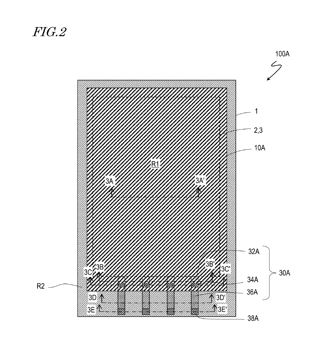
[0083]FIG. 2 is a schematic plan view of an OLED display device 10A in embodiment 1 according to the present invention.

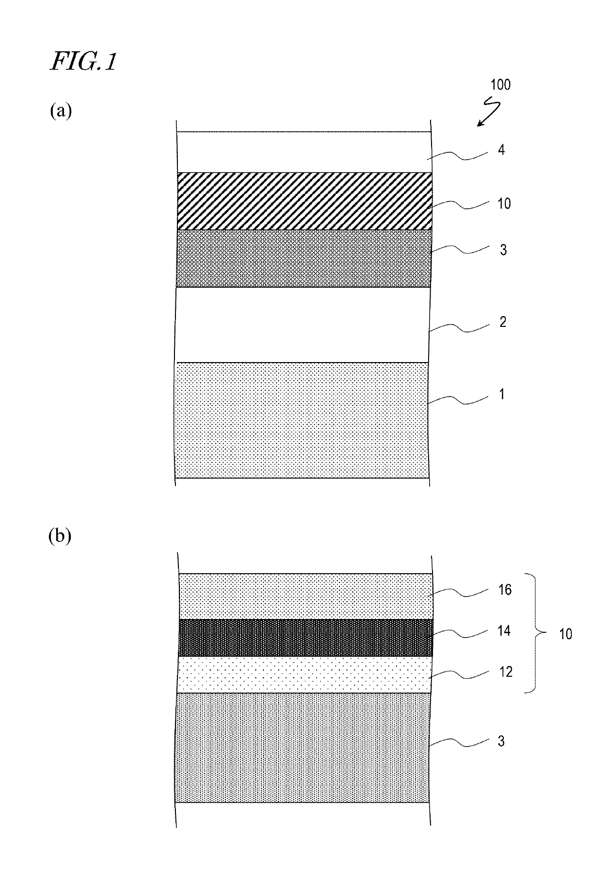
[0084]The OLED display device 100A includes the flexible substrate 1, the circuit (may be referred to as a “driving circuit” or a “back plane circuit”) 2 formed on the substrate 1, a plurality of the OLEDs 3 formed on the circuit 2, and a TFE structure 10A formed on the OLEDs 3. A layer including the plurality of OLEDs 3 may be referred to as an “OLED layer 3”. The circuit 2 and the OLED layer 3 may share a part of components. The optional polarization plate (see reference numeral 4 in FIG. 1) may further be located on the TFE structure 10A. In addition, for example, a layer having a touch panel function may be located between the TFE structure 10A and the polarization plate. Namely, the OLED d...

embodiment 2

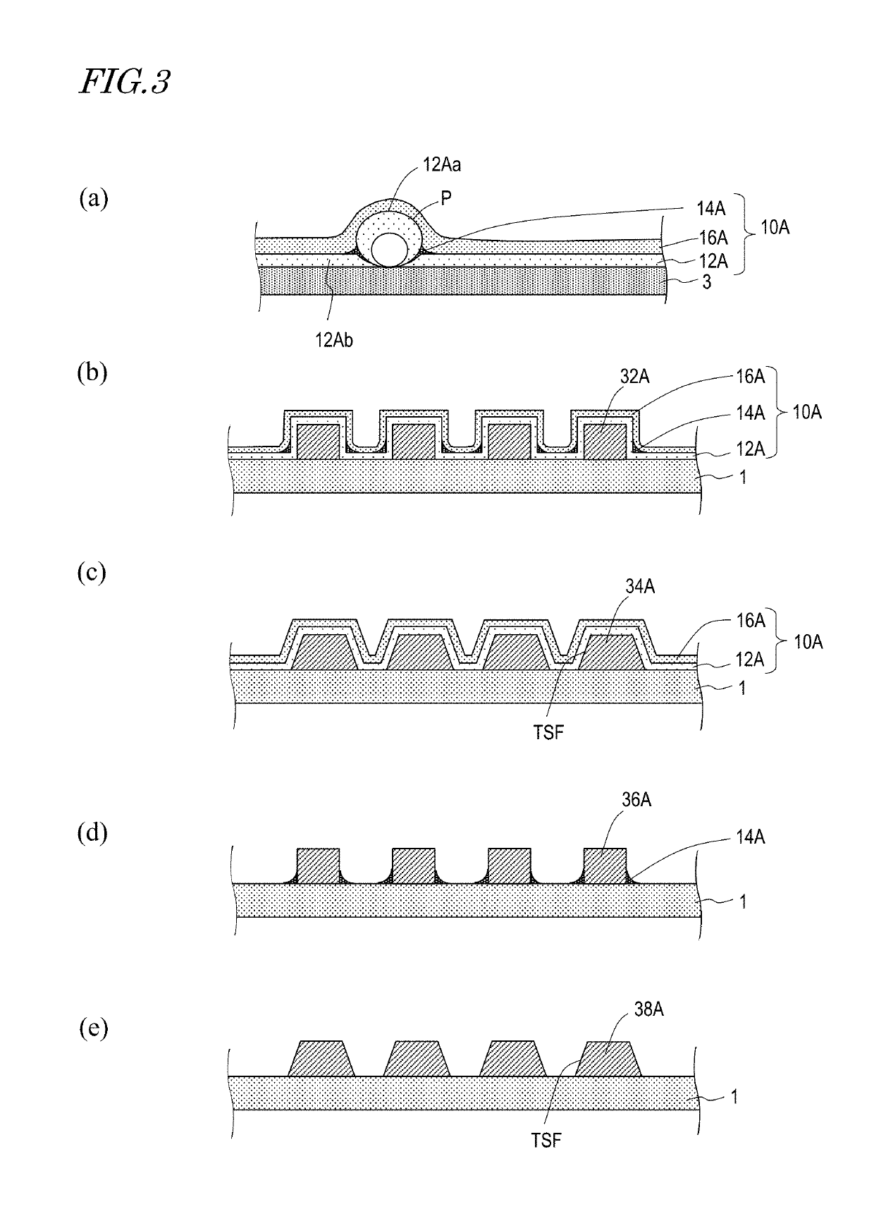
[0113]The method for producing the OLED display device in embodiment 1 includes, for example, the following steps. In at least a portion of each of the plurality of lead wires 30A, the forward tapering side surface portion is formed at least at a lowermost portion of each of two exposed side surfaces of the lead wire 30A. The forward tapering side surface portion is formed to have a tapering angle smaller than 90 degrees in a cross-section parallel to the line width direction of the lead wire 30A. Next, the first inorganic barrier layer 12A is formed selectively on the active region R1. Then, a vapor-like or mist-like acrylic monomer is supplied into the chamber. In the step of condensing the acrylic monomer on the first inorganic barrier layer 12A, the acrylic monomer is condensed so as not to be present on the portion of each lead wire 30A having the forward tapering side surface portion. The condensed acrylic monomer is irradiated with light (e.g., ultraviolet light) to form the ...


PUM


Abstract

Am organic electroluminescent device (100A) in an embodiment includes an element substrate including a plurality of organic electroluminescent elements (3) supported by a substrate; and a thin film encapsulation structure (10E) formed on the plurality of organic electroluminescent elements. The thin film encapsulation structure (10E) includes at least one complex stack body (10S) including a first inorganic barrier layer (12E), an organic barrier layer (14E) in contact with a top surface of the first inorganic barrier layer (12E) and including a plurality of solid portions discretely distributed, and a second inorganic barrier layer (16E) in contact with the top surface of the first inorganic barrier layer and a top surface of each of the plurality of solid portions of the organic barrier layer. The plurality of solid portions include a plurality of solid portions discretely provided and each having a recessed surface.

Description

TECHNICAL FIELD[0001]The present invention relates to an organic electroluminescent device (e.g., organic EL display device or organic EL illumination device) and a method for producing the same.BACKGROUND ART[0002]Organic EL (Electro-Luminescent) display devices start being put into practical use. One feature of an organic EL display device is being flexible. An organic EL display device includes, in each of pixels, at least one organic EL element (Organic Light Emitting Diode: OLED) and at least one TFT (Thin Film Transistor) controlling an electric current to be supplied to each of the at least one OLED). Hereinafter, an organic EL display device will be referred to as an “OLED display device”. Such an OLED display device including a switching element such as a TFT or the like in each of OLEDs is called an “active matrix OLED display device”. A substrate including the TFTs and the OLEDs will be referred to as an “element substrate”.[0003]An OLED (especially, an organic light emit...

Claims


Application Information

Patent Timeline
Patent Type & Authority Patents(United States)
IPC IPC(8): H01L51/56H01L51/52H01L27/32B05D1/00
CPCH01L51/5256B05D1/60H01L27/3276H01L51/56H01L2251/558H01L2227/323H01L2251/301H01L2251/5338H10K59/131H10K50/8445H10K2102/311H10K2102/351H10K50/00H10K59/00H10K71/00H10K59/1201H10K2102/00G09F9/30
Inventor KISHIMOTO, KATSUHIKO
Owner SAKAI DISPLAY PROD
Why Eureka
Try Eureka