Unlock instant, AI-driven research and patent intelligence for your innovation.

AMOLED pixel driving circuit and pixel driving method

a technology of pixel driving circuit and pixel driving method, which is applied in the direction of static indicating devices, instruments, cathode-ray tube indicators, etc., can solve the problems of increased signal lines, unstable luminescence of oled, increased cost, etc., and achieves reduced circuit structure, reduced cost, and reduced control signal amount

Inactive Publication Date: 2019-05-21
TCL CHINA STAR OPTOELECTRONICS TECH CO LTD
View PDF4 Cites 3 Cited by
  • Summary
  • Abstract
  • Description
  • Claims
  • Application Information

AI Technical Summary

Benefits of technology

This configuration achieves stable luminescence and uniform brightness by reducing the influence of threshold voltage on current flow, simplifying the circuit structure, and decreasing the number of control signals, thus lowering costs and improving efficiency.

Problems solved by technology

However, the threshold voltage of the traditional 2T1C pixel driving circuit will drift along with the working times. Thus, it results in that the luminescence of the OLED is unstable and the nonuniform luminescence and uneven brightness among the respective pixels.
The amount of the signal lines is increased to raise the loading of the control IC, which goes against the saving of the cost.

Method used


Image

  • AMOLED pixel driving circuit and pixel driving method
  • AMOLED pixel driving circuit and pixel driving method
  • AMOLED pixel driving circuit and pixel driving method

Examples


Embodiment Construction

[0076]For better explaining the technical solution and the effect of the present invention, the present invention will be further described in detail with the accompanying drawings and the specific embodiments.

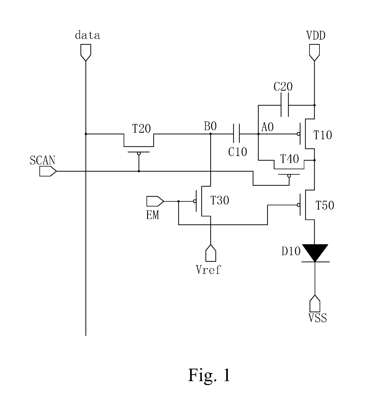
[0077]Please refer to FIG. 7 and FIG. 8, together. The present invention first provides an AMOLED pixel driving circuit. The AMOLED pixel driving circuit is the 4T2C structure, and comprises: a first thin film transistor T1, a second thin film transistor T2, a third thin film transistor T3, a fourth thin film transistor T4, a first capacitor C1, a second capacitor C2 and an organic light emitting diode D1. All the respective thin film transistors are P type thin film transistors.

[0078]the first thin film transistor T1 is a drive thin film transistor, and a gate thereof is electrically coupled to one end of the first capacitor C1 through a first node A, and a source is electrically coupled to a power source positive voltage VDD, and a drain is electrically coupled to an anode o...


PUM


Abstract

Disclosed are an AMOLED pixel driving circuit and a pixel driving method. The AMOLED pixel driving circuit utilizes the 4T2C structure, and comprises: a first thin film transistor (T1), a second thin film transistor (T2), a third thin film transistor (T3), a fourth thin film transistor (T4), a first capacitor (C1), a second capacitor (C2) and an organic light emitting diode (D1); the nth scan signal (SCAN(n)) and the n+1th scan signal (SCAN(n+1)) are combined with each other, and correspond to a threshold voltage sensing stage, a holding stage, a programming stage and a drive stage one after another. In comparison with the pixel driving circuit of the 5T2C structure, the corresponding thin film transistor is controlled merely with arranging the scan signal. There will be the compensation function, and the amount of the control signals can be decreased, and the circuit structure is simplified and the cost is decreased.

Description

FIELD OF THE INVENTION[0001]The present invention relates to an OLED display technology field, and more particularly to an AMOLED pixel driving circuit and a pixel driving method.BACKGROUND OF THE INVENTION[0002]The Organic Light Emitting Display (OLED) possesses many outstanding properties of self-illumination, low driving voltage, high luminescence efficiency, short response time, high clarity and contrast, near 180° view angle, wide range of working temperature, applicability of flexible display and large scale full color display. The OLED is considered as the most potential display device.[0003]The OLED can be categorized into two major types according to the driving methods, which are the Passive Matrix OLED (PMOLED) and the Active Matrix OLED (AMOLED), i.e. two types of the direct addressing and the Thin Film Transistor (TFT) matrix addressing. The AMOLED comprises pixels arranged in array and belongs to active display type, which has high lighting efficiency and is generally ...

Claims


Application Information

Patent Timeline
Patent Type & Authority Patents(United States)
IPC IPC(8): G09G5/00G09G3/3233G09G3/3258
CPCG09G3/3258G09G3/3233G09G2300/0426G09G2300/0819G09G2300/0852G09G2320/043G09G2300/0871G09G2310/0208G09G2310/0262G09G2320/0233G09G2300/0861
Inventor CAI, YUYING
Owner TCL CHINA STAR OPTOELECTRONICS TECH CO LTD