
MEMS microphone package

a microphone and microphone technology, applied in the field of mic package, can solve the problems of inconsistent wire bonding, etc., and achieve the effect of low profile and high sensitivity

Active Publication Date: 2019-05-21
LINGSEN PRECISION INDS
View PDF4 Cites 0 Cited by
  • Summary
  • Abstract
  • Description
  • Claims
  • Application Information

AI Technical Summary

Benefits of technology

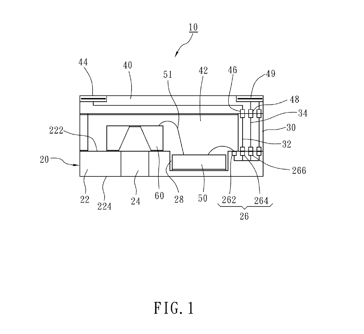
[0006]The present invention has been accomplished under the circumstances in view. It is the main object of the present invention to provide a MEMS microphone package, which has the advantages of low profile and high sensitivity.
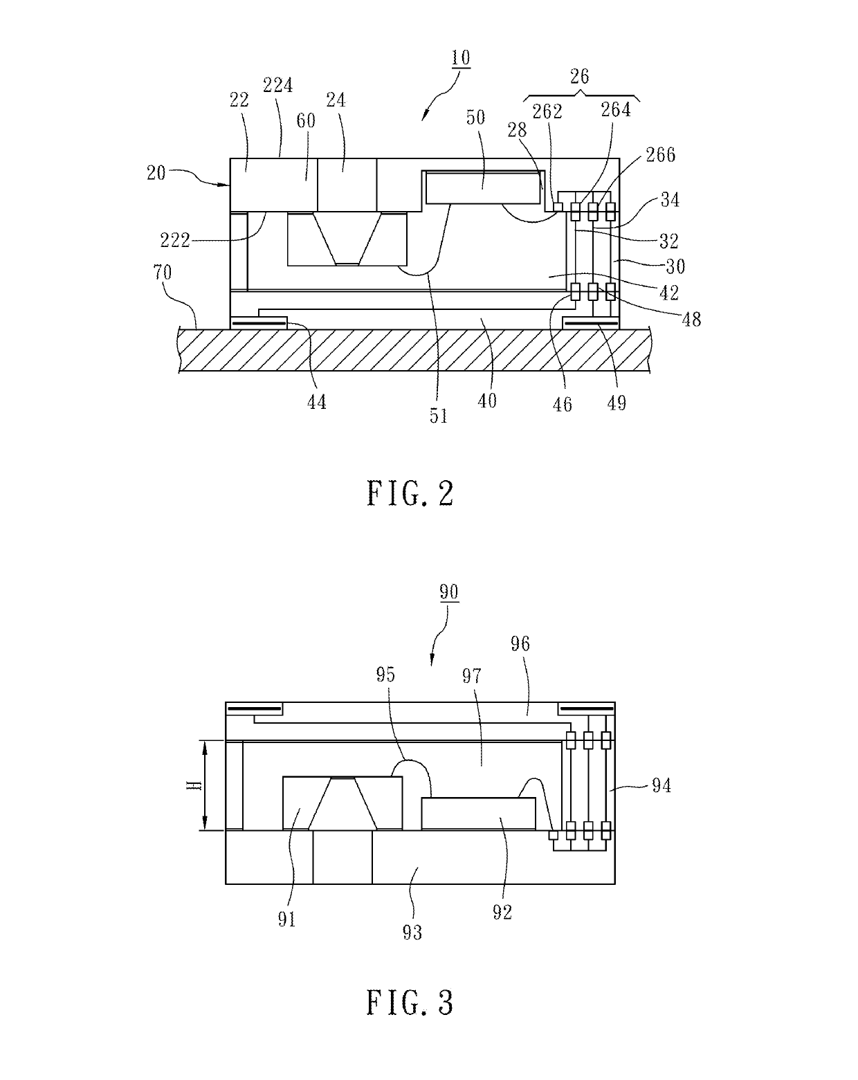
[0008]Preferably, the processor chip is electrically connected with the conduction part and the acoustic wave sensor using wire bonding technology. Thus, because the processor chip is mounted in the notch of the base layer without occupying any space of the chamber, the MEMS microphone package of the present invention can have a relatively larger back volume to enhance the sensitivity of the acoustic wave sensor. Further, the height of the metal wire between the processor chip and the acoustic wave sensor can be lowered and, the sidewall does not need to provide a spare height for accommodating the metal wire, and thus, the MEMS microphone package of the present invention has a low-profile characteristic.

Problems solved by technology

However, since MEMS microphones have been widely used in smart phones, wire bonding is obviously inconsistent with the current market trend of low profile packaging.

Method used


Image

  • MEMS microphone package
  • MEMS microphone package

Examples


Embodiment Construction

[0013]Referring to FIG. 1, a MEMS (micro-electromechanical system) microphone package 10 in accordance with the present invention is shown. The MEMS microphone package 10 comprises a substrate 20, a sidewall 30, a cover plate 40, a processor chip 50 and an acoustic wave sensor 60.

[0014]The substrate 20 comprises a base layer 22, a sound hole 24, a conduction part 26 and a notch 28. The base layer 22 defines a top surface 222 and an opposing bottom surface 224. The sound hole 24 cuts through the top surface 222 and bottom surface 224 of the base layer 22 for the passing of acoustic waves. The conduction part 26 is arranged on the base layer 22, comprising a first contact 262 and a second contact 264. The first contact 262 and the second contact 264 are disposed in conduction with each other. The notch 28 is located on the top surface 222 of the base layer 22.

[0015]The sidewall 30 has one end thereof mounted at the base layer 22, more specifically, the sidewall 30 has one end thereof ...


PUM

PropertyMeasurementUnit
temperatureaaaaaaaaaa
heightaaaaaaaaaa
conductionaaaaaaaaaa

Abstract

A MEMS microphone package includes a substrate including a base layer, a sound hole cut through opposing top and bottom surfaces of the base layer, a conduction part arranged on the base layer and a notch located on the top surface of the base layer, a sidewall connected with one end thereof to the top surface of the base layer and having a conducting line electrically connected to the conduction part, a cover plate connected to an opposite end of the sidewall and having a solder pad and a third contact disposed in conduction with the solder pad and electrically connected to the conducting line, a processor chip mounted in the notch and electrically connected to the conduction part, and an acoustic wave sensor mounted on the base layer to face toward the sound hole and electrically connected to the processor chip.

Description

BACKGROUND OF THE INVENTION1. Field of the Invention[0001]The present invention relates to semiconductor packaging technology and more particularly, to a MEMS (micro-electromechanical system) microphone package.2. Description of the Related Art[0002]MEMS is a technology that in its most general form can be defined as miniaturized mechanical and electro-mechanical elements (i.e., devices and structures) that are made using the techniques of micro fabrication. When compared with conventional electrets condenser microphones (ECM), MEMS microphones have the advantages of small package size, low power consumption and better environmental interference (such as temperature variation and electromagnetic interference) suppression ability. Therefore, the application of MEMS microphones in the field of acoustics will be more and more widespread.[0003]In a conventional MEMS microphone 90, as illustrated in FIG. 2, the acoustic wave sensor 91 and the ASIC (Application-specific Integrated Circuit...

Claims


Application Information

Patent Timeline
Patent Type & Authority Patents(United States)
IPC IPC(8): H04R25/00H04R1/04B81C1/00H04R19/04B81B7/00
CPCH04R19/04B81B7/007B81C1/0023H04R1/04H04R2201/003B81B2201/0257B81B2207/012B81B2207/095
Inventor LIAO, HSIEN-KENTU, MING-TETIAN, JYONG-YUEYEH, YAO-TING
Owner LINGSEN PRECISION INDS
Learn More