Memory device and operation method thereof

a memory device and operation method technology, applied in the field of memory devices and operation methods thereof, can solve the problem that the threshold voltage distribution of string select transistors is difficult to adjust by programming

Active Publication Date: 2019-05-28
MACRONIX INT CO LTD
View PDF8 Cites 2 Cited by
  • Summary
  • Abstract
  • Description
  • Claims
  • Application Information

AI Technical Summary

Benefits of technology

[0003]The present invention discloses a memory device and an operation method thereof, which is possible to adjust the threshold voltage of first select transistors by using pre-charge circuits.

Problems solved by technology

In some memory architectures, such as three-dimensional memory architecture, the threshold voltage distribution of the string select transistor is difficult to adjust by programming.

Method used


Image

  • Memory device and operation method thereof
  • Memory device and operation method thereof
  • Memory device and operation method thereof

Examples


first embodiment

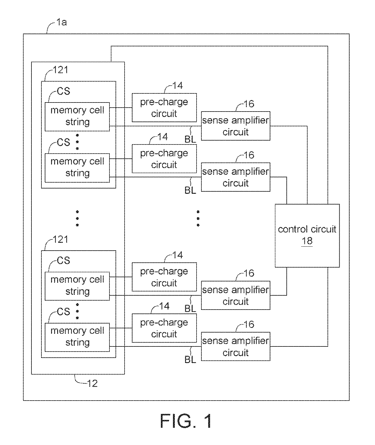
[0014]Referring to FIG. 1, FIG. 1 shows a block diagram of a memory device of the present invention. A memory device 1a includes a memory array 12, a number of bit lines BL, a number of pre-charge circuits 14, a number of sense amplifier circuits 16 and a control circuit 18.

[0015]The memory array 12 includes a number of memory blocks 121. Each memory blocks includes a number of memory cell string CS. Each memory cell string is coupled to one bit line BL and one pre-charge circuit 14.

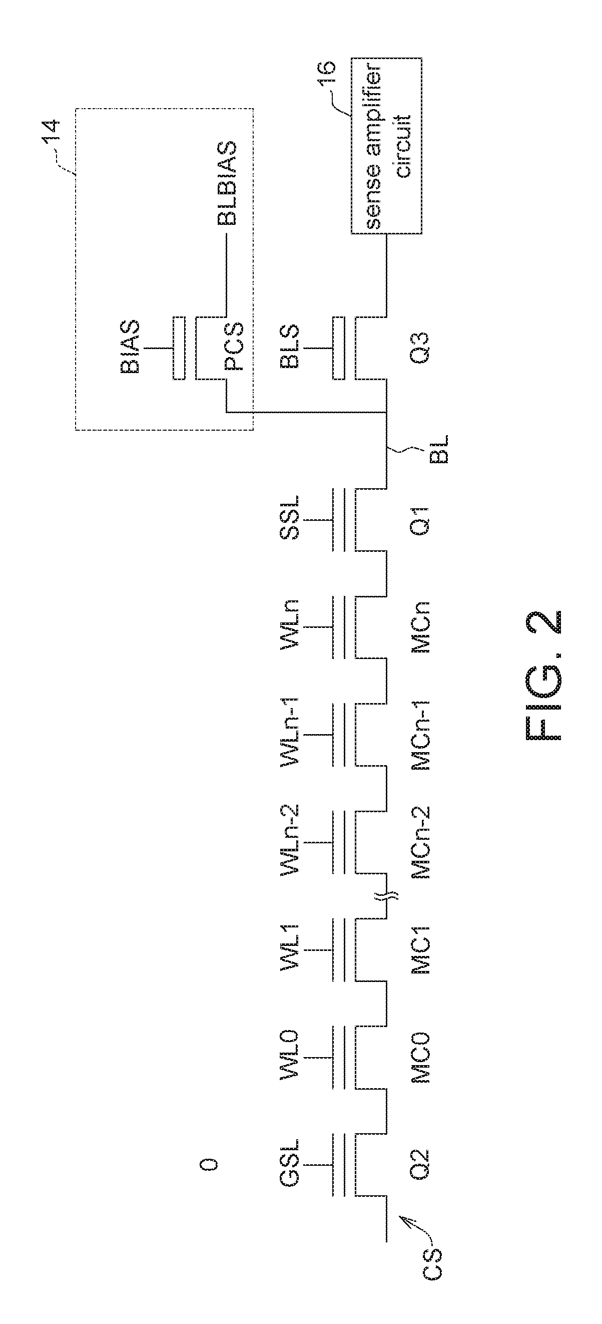
[0016]In the first embodiment, each sense amplifier circuit 16 is coupled to one memory cell string CS through one bit line BL. The control circuit 18 is coupled to the memory array 12, the bit lines BL, the pre-charge circuit 14 and the sense amplifier circuit 16. The control circuit 18 is configured to operate the memory array 12, the bit lines BL, the pre-charge circuit 14 and the sense amplifier circuit 16.

[0017]Furthermore, referring to FIG. 2, each memory cell string CS includes a first select tra...

second embodiment

[0024]Referring to FIG. 5, FIG. 5 shows a block diagram of a memory device of the present invention. The memory device 1b is similar to the memory device 1a, the differences may be described below.

[0025]In memory device 1b, each sense amplifier circuit 16 is coupled to two bit lines BL0, BL1. Each bit line BL0, BL1 is coupled to a memory cell string CS0, CS1. That is, the sense amplifier circuit 16 is coupled to two memory cell strings CS0, CS1 through two bit lines BL0, BL1, the details are shown in FIG. 6. The memory cell strings are portioned into first group and second group, e.g., according to odd or even. The third select transistors Q3 coupled to the memory cell strings CS0 of the first group are controlled by a first bit line select signal BLS0, and the third select transistors Q3 coupled to the memory cell strings CS1 of the second group are controlled by a second bit line select signal BLS1. The pre-charge switch PCS coupled to the memory cell strings CS0 of the first gro...


PUM


Abstract

A memory device includes a memory array including a number of memory cell strings, a number of bit lines, a number of pre-charge circuits coupled to the memory cell strings, and a number of sense amplifier circuits coupled to the memory cell strings through the bit lines. Each memory cell string includes at least one first select transistor, a second select transistor and at least one memory cell. Each bit line includes a third select transistor, and is coupled to a memory cell string. During a pre-charging stage, the pre-charge circuits provide a first voltage to pre-charge the memory cell strings. During a programming stage, for the memory cell strings to be inhibited, the sense amplifier circuits provide a second voltage lower than the first voltage. For the memory cell strings to be programmed, the sense amplifier circuits provide a third voltage lower than the second voltage.

Description

BACKGROUND OF THE INVENTIONField of the Invention[0001]The invention relates to memory device and operation method thereof. Especially, the invention relates to memory device comprising pre-charge circuit and operation method thereof.Description of the Related Art[0002]A memory device is one of important hardware component in a computer device. The memory device typically contains a plurality of memory cell strings, each memory cell string typically comprising a plurality of memory cells and at least one string select transistor for connecting a string select line (SSL). The string selection transistor is typically disposed between the memory cell and the sense amplifier circuit. In some memory architectures, such as three-dimensional memory architecture, the threshold voltage distribution of the string select transistor is difficult to adjust by programming. However, the threshold voltage distribution of the sting select transistor will affect the threshold voltage distribution of ...

Claims


Application Information

Patent Timeline
Patent Type & Authority Patents(United States)
IPC IPC(8): G11C16/04G11C7/06G11C11/4096G11C11/4074G11C16/12G06F13/40G11C7/12
CPCG11C16/12G11C11/4074G11C11/4096G11C16/0483G11C7/06G06F13/4004G11C7/12G11C16/24G11C16/26G11C7/062
Inventor CHIANG, CHIH-HELIU, YI-CHING
Owner MACRONIX INT CO LTD
Why Eureka
Try Eureka