Wimpy device by selective laser annealing

Inactive Publication Date: 2018-02-22
ELPIS TECH INC
View PDF0 Cites 3 Cited by
  • Summary
  • Abstract
  • Description
  • Claims
  • Application Information

AI Technical Summary

Benefits of technology

[0004]In accordance with an embodiment of the present principles, a method for co-integrating wimpy and nominal devices includes growing source/drain regions on semiconductor material adjacent to a gate structure to form device structures with a non-electrically active material. Selected device structures are masked with a block mask. Unmasked device structures are selectively annealed to increase electrical activity of the non-electrically active material to adjust a threshold voltage between the selected device structures and the unmasked device structures.
[0005]Another method for co-integrating wimpy and nominal devices includes forming fins on or in a substrate; forming a gate structure over the fins; growing source/drain regions on the fins adjacent to the gate structure to form

Problems solved by technology

As devices scale down, making wimpy devices with larger Lg and a same contacted gate (poly) pitch (CPP) as

Method used


Image

  • Wimpy device by selective laser annealing
  • Wimpy device by selective laser annealing
  • Wimpy device by selective laser annealing

Examples


Embodiment Construction

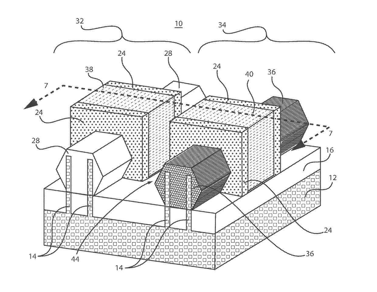
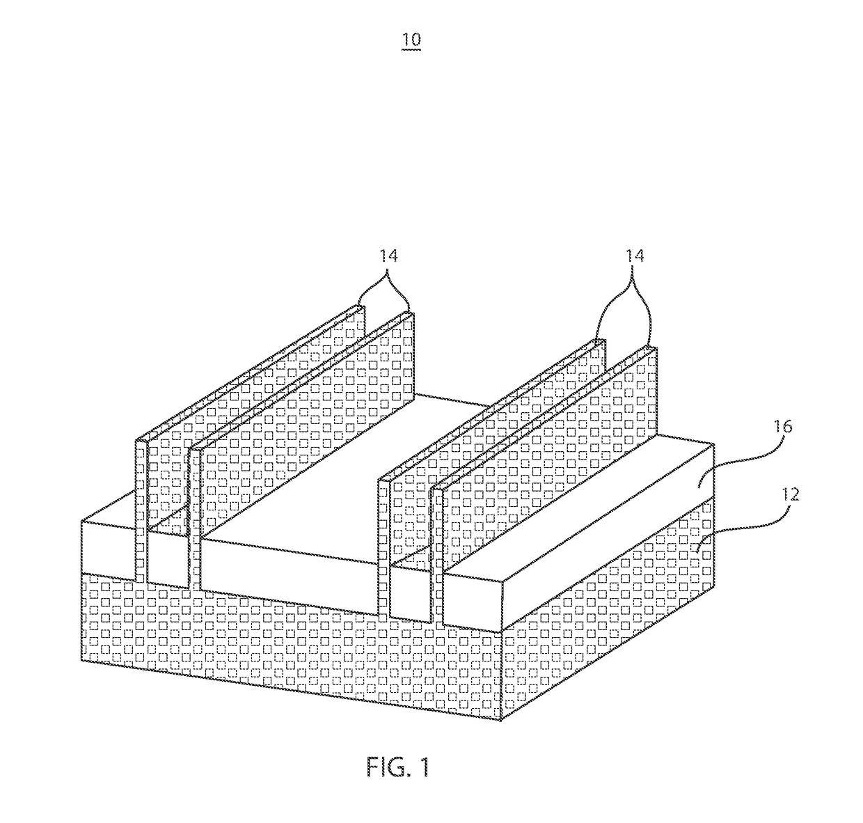
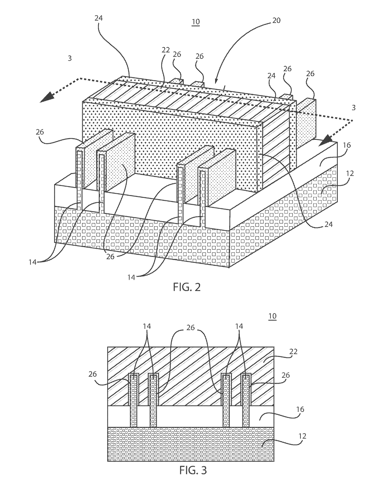
[0017]In accordance with the present principles, devices and methods are provided for forming wimpy devices with a same gate length (Lg), contacted gate (poly) pitch (CPP), and a same channel doping as nominal devices to save design and processing costs. In accordance with useful embodiments, wimpy and nominal devices are formed concurrently and include similar structure and materials.

[0018]In one particularly useful embodiment, source / drain epitaxial growth is performed in a phosphine environment. Si3P4 is formed when an overabundance of phosphine flows into a process gas during a fast growing low temperature epitaxial silicon process. The Si3P4 compound gets incorporated into the silicon lattice and creates a tensile strain (as compared with the underlying silicon substrate lattice, e.g., on a planar substrate or a fin). The phosphorus is chemically bonded and not electrically active (e.g., an overall phosphorus concentration may be about 4×10²¹ atoms, but only 2×10²⁰-3×10²⁰ phosp...


PUM


Abstract

A method for co-integrating wimpy and nominal devices includes growing source/drain regions on semiconductor material adjacent to a gate structure to form device structures with a non-electrically active material. Selected device structures are masked with a block mask. Unmasked device structures are selectively annealed to increase electrical activity of the non-electrically active material to adjust a threshold voltage between the selected device structures and the unmasked device structures.

Description

BACKGROUNDTechnical Field[0001]The present invention generally relates to semiconductor processing, and more particularly to methods and devices having a combination of wimpy and nominal devices integrated together by employing a selective anneal, e.g., laser annealing.Description of the Related Art[0002]Devices in non-critical circuit paths are preferred to have larger threshold voltages (Vt) than nominal devices. This assists in maintaining low leakage rates while not compromising circuit performance. These devices with larger Vt are called ‘wimpy’ devices. Conventionally, wimpy devices are made with larger gate lengths (Lg) and have higher channel doping than the nominal devices. These features employ special device and mask designs and require additional steps of lithography and implantation.[0003]As devices scale down, making wimpy devices with larger Lg and a same contacted gate (poly) pitch (CPP) as for the nominal devices is impractical because there is very little room for ...

Claims


Application Information

Patent Timeline
IPC IPC(8): H01L21/8234H01L29/267H01L29/66H01L21/268H01L21/324H01L29/24H01L27/088H01L29/78H01L29/08
CPCH01L29/267H01L29/66545H01L21/268H01L21/324H01L21/823431H01L27/0886H01L21/823418H01L29/7848H01L29/0847H01L29/24H01L21/845H01L27/088
Inventor CHENG, KANGGUOLOUBET, NICOLAS J.MIAO, XINREZNICEK, ALEXANDER
Owner ELPIS TECH INC
Why Eureka
Try Eureka