Supercharge Your Innovation With Domain-Expert AI Agents!

Organic light emitting diode and organic light emitting diode display including the same

a light emitting diode and organic technology, applied in the direction of basic electric elements, electrical equipment, semiconductor devices, etc., can solve the problems of thermal evaporation method being difficult to apply in a large area apparatus, the response speed is limited, and the damage to the organic light emitting diode at the time of forming a cathode may be reduced or prevented, and the light emitting efficiency of the blue light emission layer may be increased.

Active Publication Date: 2019-05-28
SAMSUNG DISPLAY CO LTD
View PDF13 Cites 0 Cited by
  • Summary
  • Abstract
  • Description
  • Claims
  • Application Information

AI Technical Summary

Benefits of technology

The present patent aims to provide an organic light emitting diode (OLED) that has high light emitting efficiency in a large area device. The patent discusses a method of forming an electron injection layer with a dipolar material and metal to increase light emitting efficiency. Additionally, a buffer layer with low work function metal can be included between the cathode and electron injection layer to prevent damage to the OLED during the sputtering process. Furthermore, a blue light emission layer can be enhanced by adding an auxiliary layer to increase light emitting efficiency. Overall, the patent describes methods to improve stability and efficiency of OLEDs in large area devices.

Problems solved by technology

However, the LCD is a light-emitting / receiving device requiring a separate backlight and has limitations in view of a response speed, a viewing angle, and the like.
However, the thermal evaporation method has a difficulty of being applied in a large area apparatus due to a warpage phenomenon of a glass and a mask.

Method used


Image

  • Organic light emitting diode and organic light emitting diode display including the same
  • Organic light emitting diode and organic light emitting diode display including the same
  • Organic light emitting diode and organic light emitting diode display including the same

Examples


Embodiment Construction

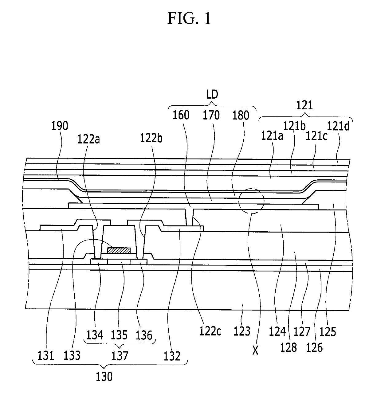
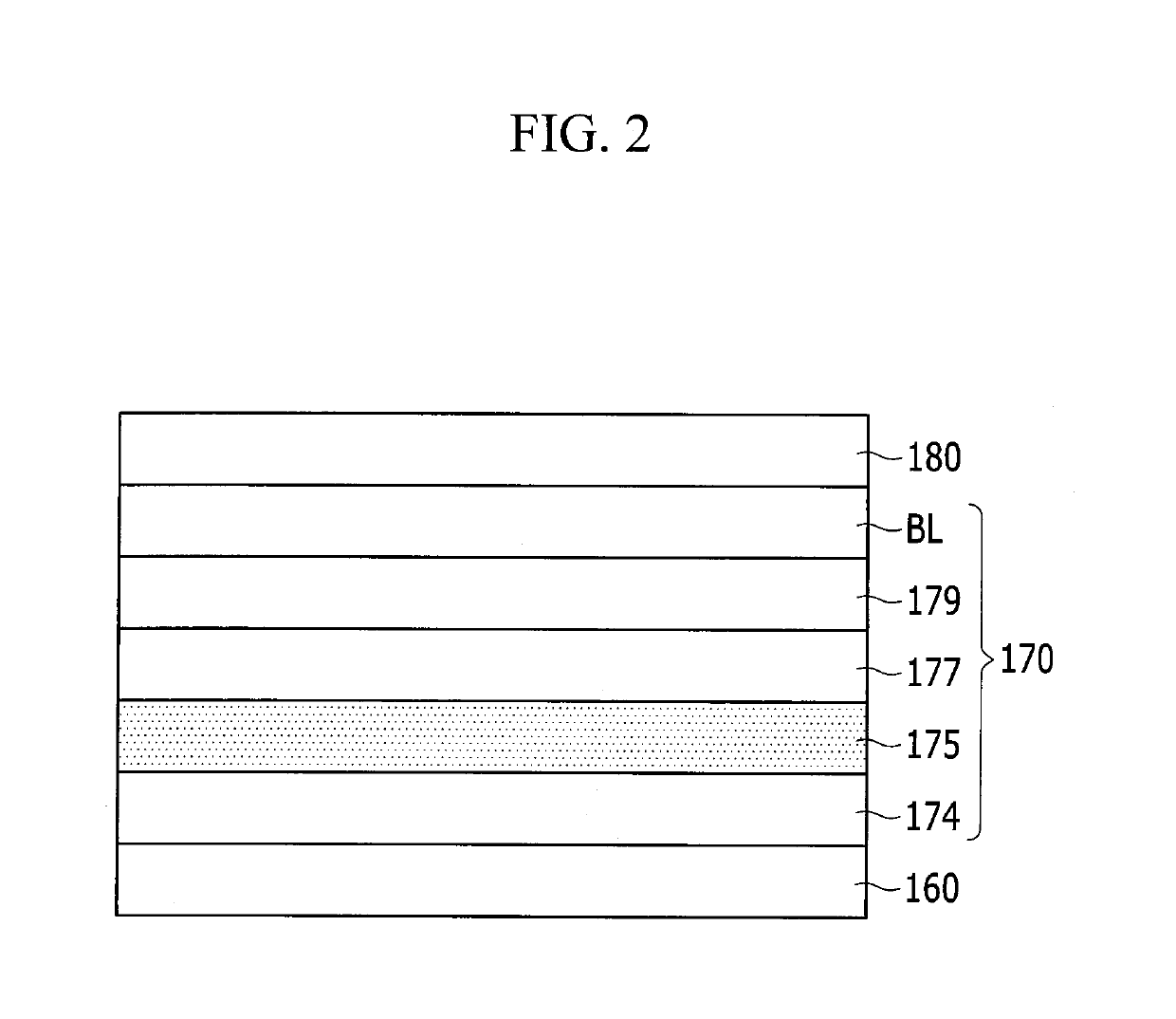
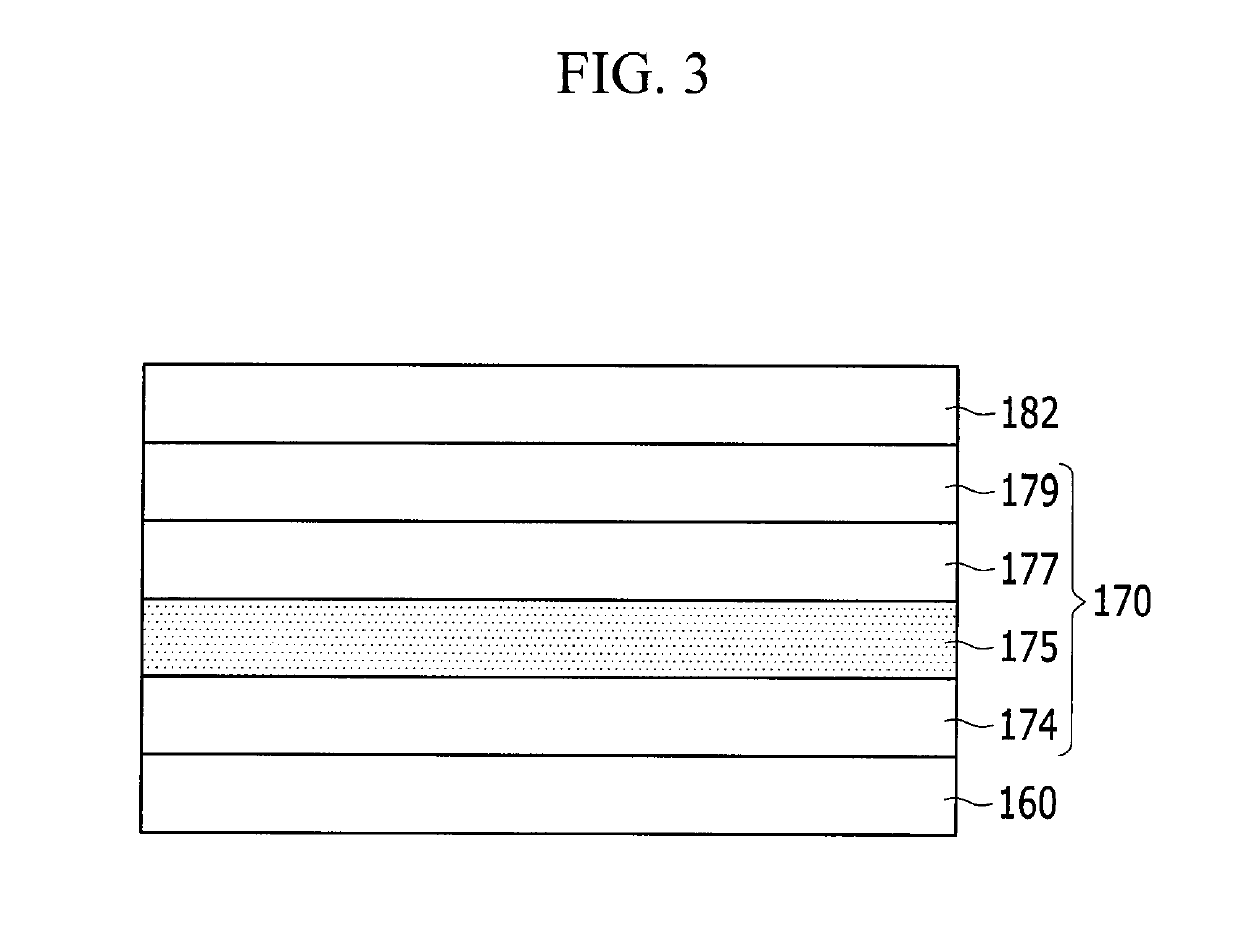
[0048]Hereinafter, example embodiments of the present disclosure will be described in detail with reference to the accompanying drawings. However, the present disclosure is not limited to the example embodiments which are described herein, and may be modified in various different ways. Indeed, the example embodiments of the present disclosure described below are provided so as to provide a thorough and complete description and fully convey the spirit of the present disclosure to those skilled in the art.

[0049]In the drawings, thicknesses of layers and regions may be exaggerated for clarity. In addition, in the context of the present application, in the case in which it is stated that a layer is present ‘on’ another layer or a substrate, the layer may be directly on the other layer or the substrate or be indirectly on the other layer or substrate and have other layers interposed therebetween. Further, in the context of the present application, when a first element is referred to as b...


PUM


Abstract

An organic light emitting diode includes: a first electrode; a second electrode facing the first electrode; a light emission layer between the first electrode and the second electrode; an electron injection layer between the second electrode and the light emission layer; and a buffer layer between the electron injection layer and the second electrode, where the electron injection layer includes a dipolar material and a first metal, and the buffer layer includes a metal having a work function of 4.0 eV or less.

Description

CROSS-REFERENCE TO RELATED APPLICATION[0001]This application claims priority to and the benefit of Korean Patent Application No. 10-2015-0008682 filed in the Korean Intellectual Property Office on Jan. 19, 2015, the entire contents of which are incorporated herein by reference.BACKGROUND[0002]1. Field[0003]Embodiments of the present disclosure relate to an organic light emitting diode and an organic light emitting diode display including the same.[0004]2. Description of the Related Art[0005]Recently, monitors, televisions, and the like, have been made to have light weight and thin thickness. In accordance with recent demand, cathode ray tube (CRT) displays have been replaced with liquid crystal displays (LCD). However, the LCD is a light-emitting / receiving device requiring a separate backlight and has limitations in view of a response speed, a viewing angle, and the like. An organic light emitting diode display in which a viewing angle is wide, contrast is excellent, and a response ...

Claims


Application Information

Patent Timeline
Patent Type & Authority Patents(United States)
IPC IPC(8): H01L51/52H01L51/00H01L51/50H10K99/00
CPCH01L51/0061H01L51/0059H01L51/5092H01L51/5265H01L51/5231H01L51/0074H01L51/0072H01L51/0073H10K59/12H10K50/171H10K59/876H10K59/80523H10K85/631H10K85/657H10K85/636H10K50/826H10K50/852H10K85/6572H10K85/6574H10K85/6576
Inventor YOON, SEOK GYUKIM, DONG CHANKIM, EUNG DOJUNG, BO RAHWANG, KYU HWANKIM, SUNG CHULKIM, WON-JONGSONG, YOUNG-WOOLEE, JONG HYUK
Owner SAMSUNG DISPLAY CO LTD
Features
  • R&D
  • Intellectual Property
  • Life Sciences
  • Materials
  • Tech Scout
  • Unparalleled Data Quality
  • Higher Quality Content
  • 60% Fewer Hallucinations
Learn More