Light emitting device and method of manufacturing the same

a technology of light emitting device and manufacturing method, which is applied in the direction of discharge tube/lamp details, discharge tube luminescnet screen, organic semiconductor device, etc., can solve the problems of uneven intra-plane electric potential distribution, high film resistance of transparent electrode, fluctuation of luminance, etc., to increase the amount of light, increase film resistance, and increase the effect of ligh

Inactive Publication Date: 2009-08-25
SEMICON ENERGY LAB CO LTD
View PDF166 Cites 48 Cited by
  • Summary
  • Abstract
  • Description
  • Claims
  • Application Information

AI Technical Summary

Benefits of technology

[0011]Compared to the downward emission structure, the number of material layers through which light emitted from the organic compound-containing layer passes is smaller in the upward emission structure and stray light caused between material layers of different refractive indexes is accordingly reduced.
[0012]Not all of light generated in the organic compound layer are taken out in the direction toward the TFT from the transparent electrode serving as the cathode. For example, light emitted in the lateral direction (the direction parallel to the substrate face) is not taken out and therefore is a loss. An object of the present invention is to provide a light emitting device structured so as to increase the amount of light which is taken out in a certain direction after emitted from a light emitting element, as well as a method of manufacturing this light emitting device.
[0013]A problem of the upward emission structure is that its transparent electrode has high film resistance. The film resistance becomes even higher when the thickness of the transparent electrode is reduced. When the transparent electrode that serves as an anode or a cathode is high in film resistance, a voltage drop makes the intra-plane electric potential distribution uneven and the luminance becomes fluctuated among light emitting elements. Another object of the present invention is therefore to provide a light emitting device structured so as to lower the film resistance of a transparent electrode in a light emitting element, as well as a method of manufacturing the light emitting device. Still another object of the present invention is to provide an electric appliance that uses this light emitting device as its display unit.

Problems solved by technology

For example, light emitted in the lateral direction (the direction parallel to the substrate face) is not taken out and therefore is a loss.
A problem of the upward emission structure is that its transparent electrode has high film resistance.
When the transparent electrode that serves as an anode or a cathode is high in film resistance, a voltage drop makes the intra-plane electric potential distribution uneven and the luminance becomes fluctuated among light emitting elements.

Method used


Image

  • Light emitting device and method of manufacturing the same
  • Light emitting device and method of manufacturing the same
  • Light emitting device and method of manufacturing the same

Examples


embodiment mode 1

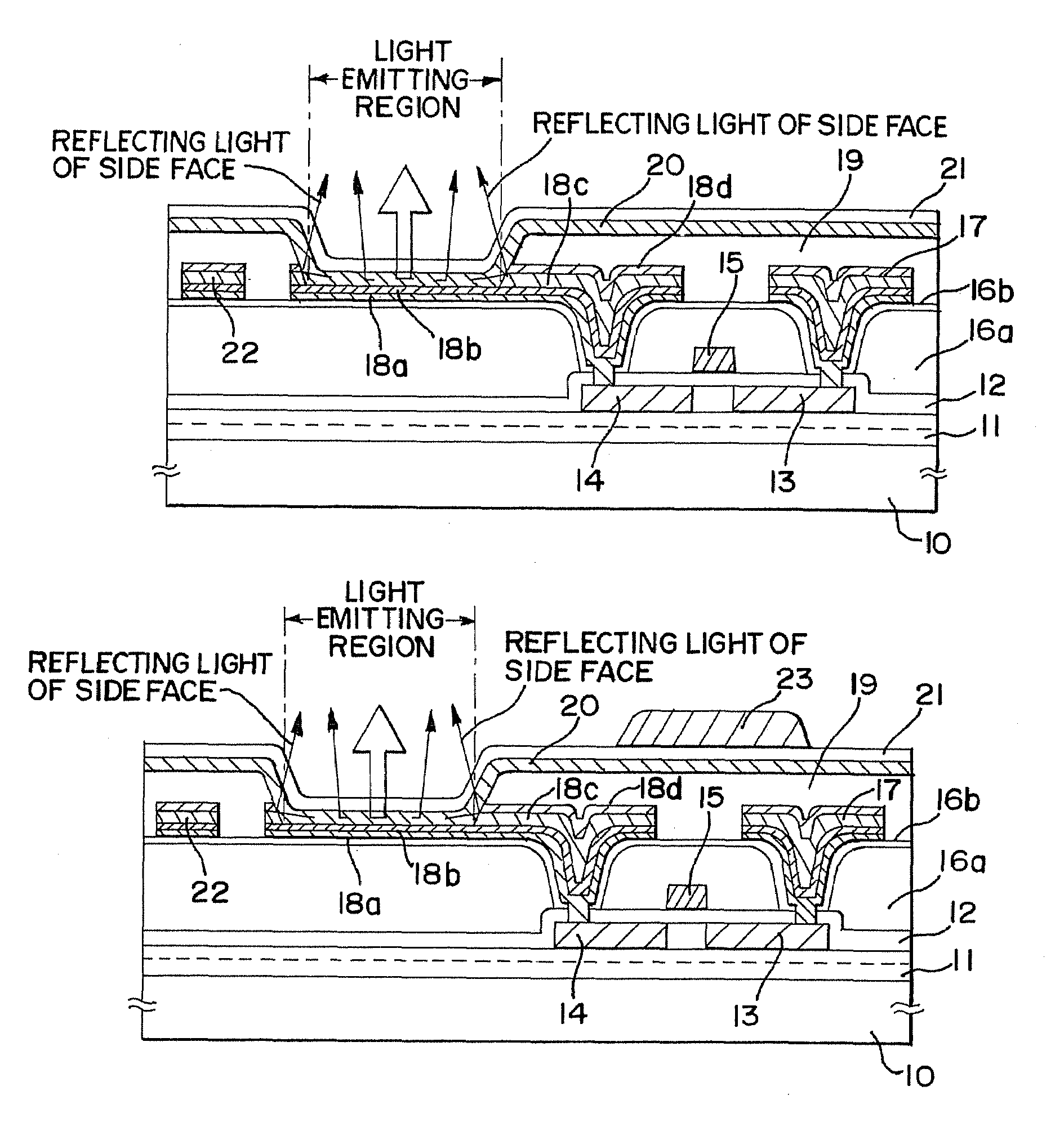
[0079]FIG. 1A is a sectional view of an active matrix light emitting device (a part of one pixel). Described here as an example is a light emitting element which uses as its light emitting layer an organic compound-containing layer formed of a high molecular weight material that emits white light.

[0080]In FIG. 1A, a TFT (p-channel TFT) on a substrate 10 having an insulating surface is an element for controlling a current flowing into an EL layer 20 that emits white light. Of regions denoted by 13 and 14, one is a source region and the other is a drain region. A base insulating film 11 (here a laminate of an insulating nitride film as a lower layer and an insulating oxide film as an upper layer) is formed on the substrate 10. A gate insulating film 12 is placed between a gate electrode 15 and an active layer of the TFT. Denoted by 16a is an interlayer insulating film formed of an organic material or an inorganic material. Reference symbol 16b represents a protective film formed of si...

embodiment mode 2

[0096]A method of combining a white color luminescent element and a color filter (hereinafter, referred to as color filter method) will be explained in reference to FIG. 5A as follows.

[0097]The color filter method is a system of forming a light emitting element having an organic compound film displaying white color luminescence and passing the provided white color luminescence through a color filter to thereby achieve luminescence of red, green, and blue.

[0098]Although there are various methods of achieving white color luminescence, a case of using a luminescent layer comprising a high molecular material formable by coating will be explained here. In this case, doping of a color pigment to the high molecular material for constituting a luminescent layer can be carried out by preparing a solution and can extremely easily be achieved in comparison with a vapor deposition method for carrying out common vapor deposition for doping a plurality of color pigments.

[0099]Specifically, after ...

embodiment mode 3

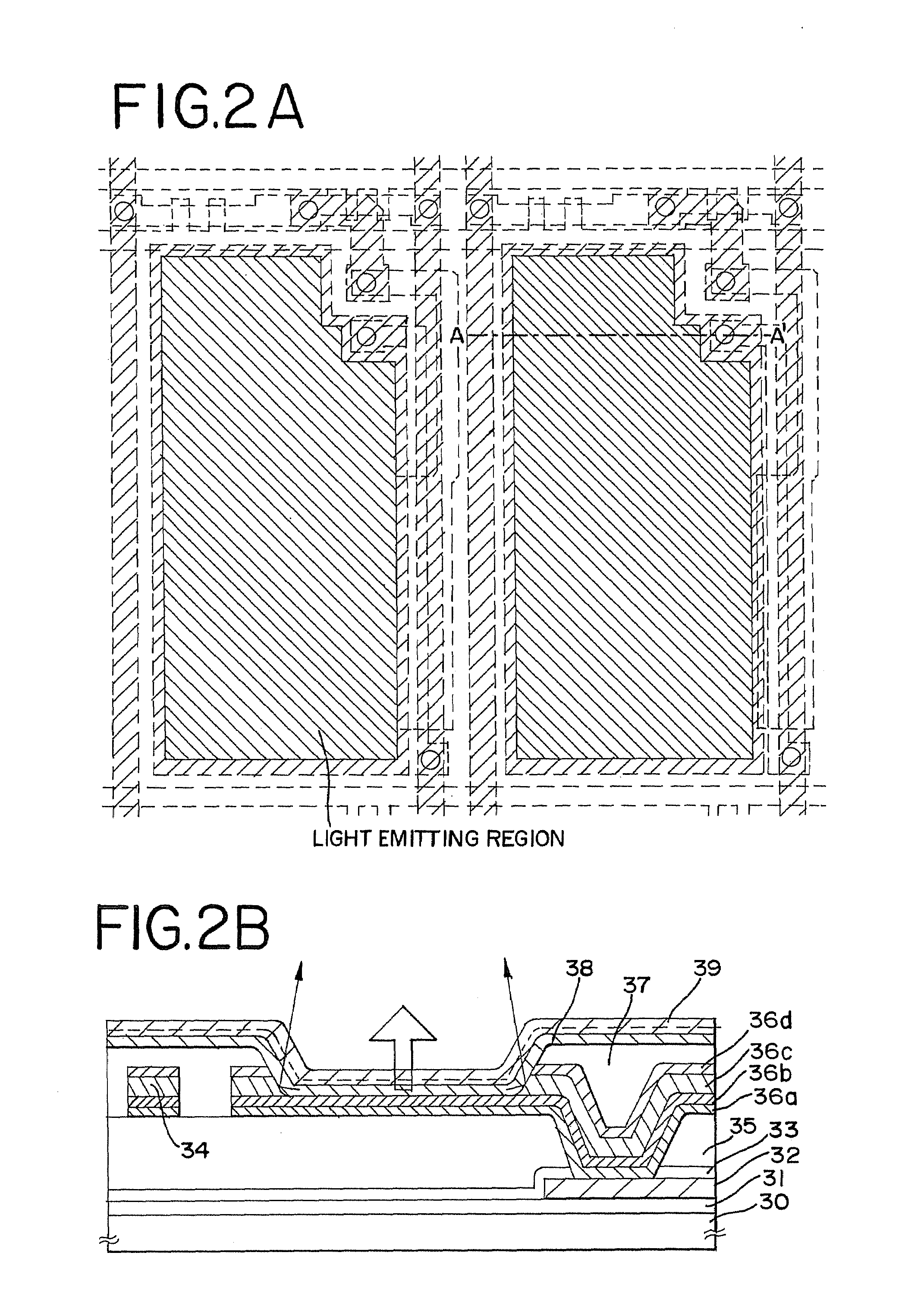
[0113]Here, a total of an EL module and arrangement of a drying agent will be explained in reference to FIG. 4. FIG. 4A is a top view of the EL module. FIG. 4B is a part of a cross-sectional view.

[0114]A substrate provided with numerous TFTs (also referred to as TFT substrate) is provided with a pixel portion 40 for display, driver circuits 41a and 41b for driving respective pixels of the pixel portion, a connecting portion for connecting the electrode provided over the EL layer and an extended wiring, a terminal portion 42 for pasting FPC for connecting to outside circuit and a drying agent 44. Further, the drying agent may be arranged such that a total of the driver circuits is concealed by the drying agent as shown by FIG. 4C although the drying agent is arranged to overlap a portion thereof in FIG. 4A and FIG. 4B. Further, the constitution is hermetically sealed by the substrate for sealing the EL element and a seal member 49. Further, FIG. 4B is a sectional view when the consti...


PUM


Abstract

All lights generated in an organic compound layer are not taken out towards a TFT from a cathode as a transparent electrode. For instance, the light is emitted in a lateral direction (direction parallel to the substrate surface) but the light emitted in the lateral direction is not taken out resultantly, which leads to a loss. Therefore, a light emitting device structured so as to increase the amount of light taken out in a certain direction is provided as well as a method of manufacturing this light emitting device. As a result of etching treatment, an upper edge portion of an insulator (19) is curved to have a radius of curvature, a slope is formed along the curved face while partially exposing layers (18c and 18d) of a first electrode, and a layer (18b) of the first electrode is exposed in a region that serves as a light emitting region. Light emitted from an organic compound layer (20) is reflected by the slope of the first electrode (layers 18c and 18d) to increase the total amount of light taken out in the direction indicated by the arrow in FIG. 1A.

Description

BACKGROUND OF THE INVENTION[0001]1. Field of the Invention[0002]The present invention relates to a light emitting device with a light emitting element that emits fluorescent light or phosphorescent light upon application of electric field to a pair of electrodes of the element which sandwich a layer containing an organic compound (hereinafter, an organic compound film), and to a method of manufacturing the light emitting device. In this specification, the term light emitting device includes an image display device, a light emitting device and a light source (including illuminating device). Also, the following modules are included in the definition of the light emitting device: a module obtained by attaching to a light emitting device a connector such as an FPC (flexible printed circuit; terminal portion), a TAB (tape automated bonding) tape, or a TCP (tape carrier package); a module in which a printed wiring board is provided at an end of the TAB tape or the TCP; and a module in whi...

Claims


Application Information

Patent Timeline
Patent Type & Authority Patents(United States)
IPC IPC(8): H05B33/00H01L27/32H01L51/52
CPCH01L27/3246H01L27/3206H01L51/5271H01L27/322H01L27/3276H01L51/5203H01L51/5221H01L51/5237H01L2251/5315H01L51/5206H10K59/38H10K59/122H10K59/131H10K50/813H10K50/818H10K50/824H10K50/828H10K50/841H10K50/844H10K50/856H10K2102/3026H10K59/30H10K50/82H10K50/84
Inventor YAMAZAKI, SHUNPEISEO, SATOSHIKUWABARA, HIDEAKI
Owner SEMICON ENERGY LAB CO LTD
Why Eureka
Try Eureka