

Magneto-resistance effect element, magnetic head, magnetic recording device and magnetic memory
- Summary
- Abstract
- Description
- Claims
- Application Information
AI Technical Summary
Benefits of technology
Problems solved by technology
Method used
Image

Examples
first embodiment
sistance Effect Element
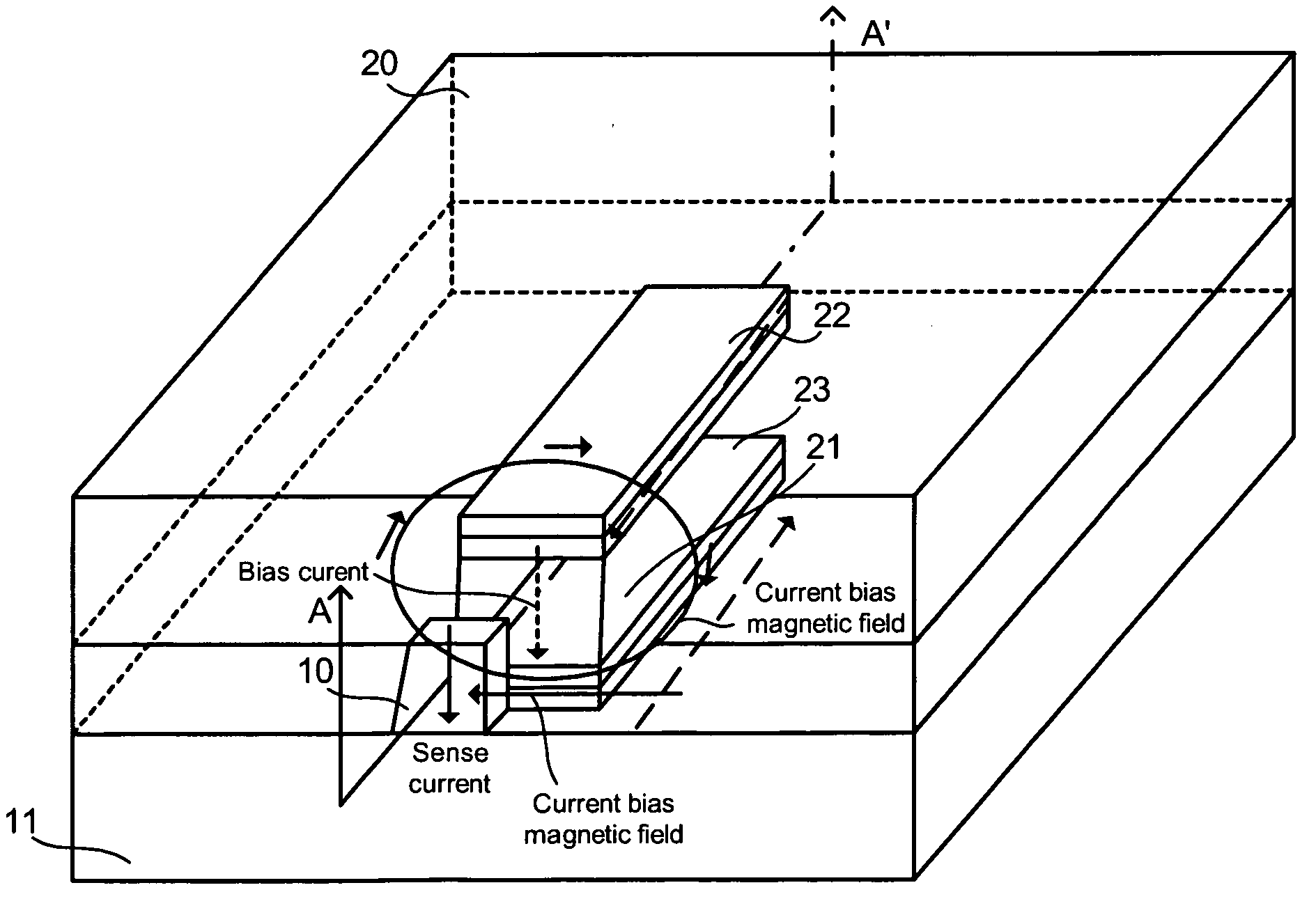
[0061]FIGS. 4 to 6 relate to the concrete structure of the magneto-resistance effect element wherein a current bias generating portion 21 is provided for the above-described magneto-resistance effect element as a fundamental structure. In these drawings, for simplification, the bottom electrode 11 and the top electrode 20 are omitted so that only the MR film 10 is represented as the magneto-resistance effect element. Since the current bias generating portion 21 applies a magnetic field to the spacer layer 15, the spacer layer 15 is concretely depicted in the MR film 10.
[0062]As shown in FIGS. 4 to 6, the current bias generating portion 21 is formed as a platy structure. In FIG. 4, the current bias generating portion 21 (platy structure) is disposed adjacent to the side surface of the magneto-resistance effect element so that the current is flowed therein along the thickness direction (from the top side to the bottom side). In this case, the clockwise bias magn...
example 1
[0081]Example 1 relating to the magneto-resistance effect element as shown in FIG. 4 (7) will be described. In Example 1, the magneto-resistance effect element was formed as follows:
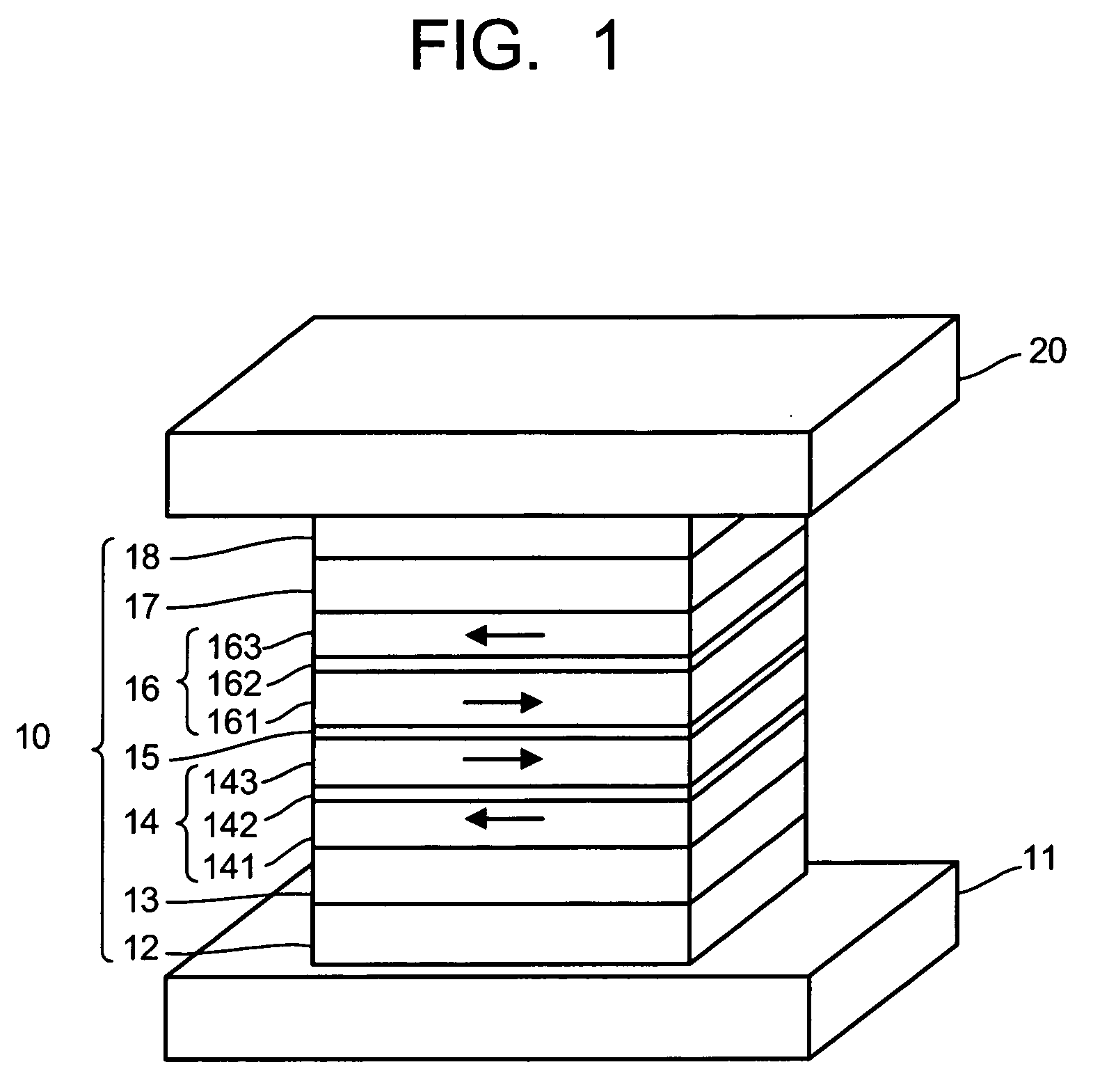
[0082]Bottom electrode 11: NiFe 1.5 μm
[0083]Underlayer 12 (buffer layer 12a / seed layer 12b): Ta 5 nm / Ru 2 μm
[0084]Pinning layer 13: PtMn 15 nm
[0085]Pinned layer 14 (pinned layer 141 / magnetic coupling layer 142 / pinned layer 143): CoFe 3 nm / Ru 0.9 nm / CoFe 3 nm
[0086]Spacer layer 15: TiOx 2 nm
[0087]Pinned layer 16 (pinned layer 161 / magnetic coupling layer 162 / pinned layer 163): CoFe 3 nm / Ru 0.9 nm / CoFe 3 nm
[0088]Pinning layer 17: PtMn 15 nm
[0089]Cap layer 18: Ta 5 nm
[0090]Current bias generating portion 21: Ti 50 nm
[0091]The above-described layers were subsequently formed except the top electrode to form the laminated body, and then, thermally treated at 290° C. for four hours under a magnetic field of 10 kOe so as to enhance the crystallinity of the laminated body and the regularization of the pinning layer...
PUM
 Abstract
Description
Claims
Application Information