Magnetoresistance effect device

a technology of magnetoresistance and effect, which is applied in the field of magnetoresistance effect devices, can solve the problems of reducing the effect of protective film on the protection device from oxidation, reducing the rate of change of magnetoresistance of the device, and reducing the output of the head, etc., and achieves excellent characteristics and good characteristics

Inactive Publication Date: 2006-06-20
TDK CORPARATION
View PDF35 Cites 1 Cited by
  • Summary
  • Abstract
  • Description
  • Claims
  • Application Information

AI Technical Summary

Benefits of technology

[0023]By means of the above, a magnetoresistance effect device and a magnetoresistance effect sensor used in, a magnetoresistance detection system and magnetic storage system can be obtained whereby excellent characteristics are obtained in regard to output value, output waveform, and bit error rate and which can provide good characteristics also in regard to thermal reliability.

Problems solved by technology

Since the current flowing through the protective film does not contribute to a change of the magnetoresistance, the rate of change of magnetoresistance of the device is decreased, diminishing the output of the head.
On the other hand, if the film thickness is small, the effectiveness of the protective film in protecting the magnetoresistance device from oxidation is decreased.

Method used


Image

  • Magnetoresistance effect device
  • Magnetoresistance effect device
  • Magnetoresistance effect device

Examples


Embodiment Construction

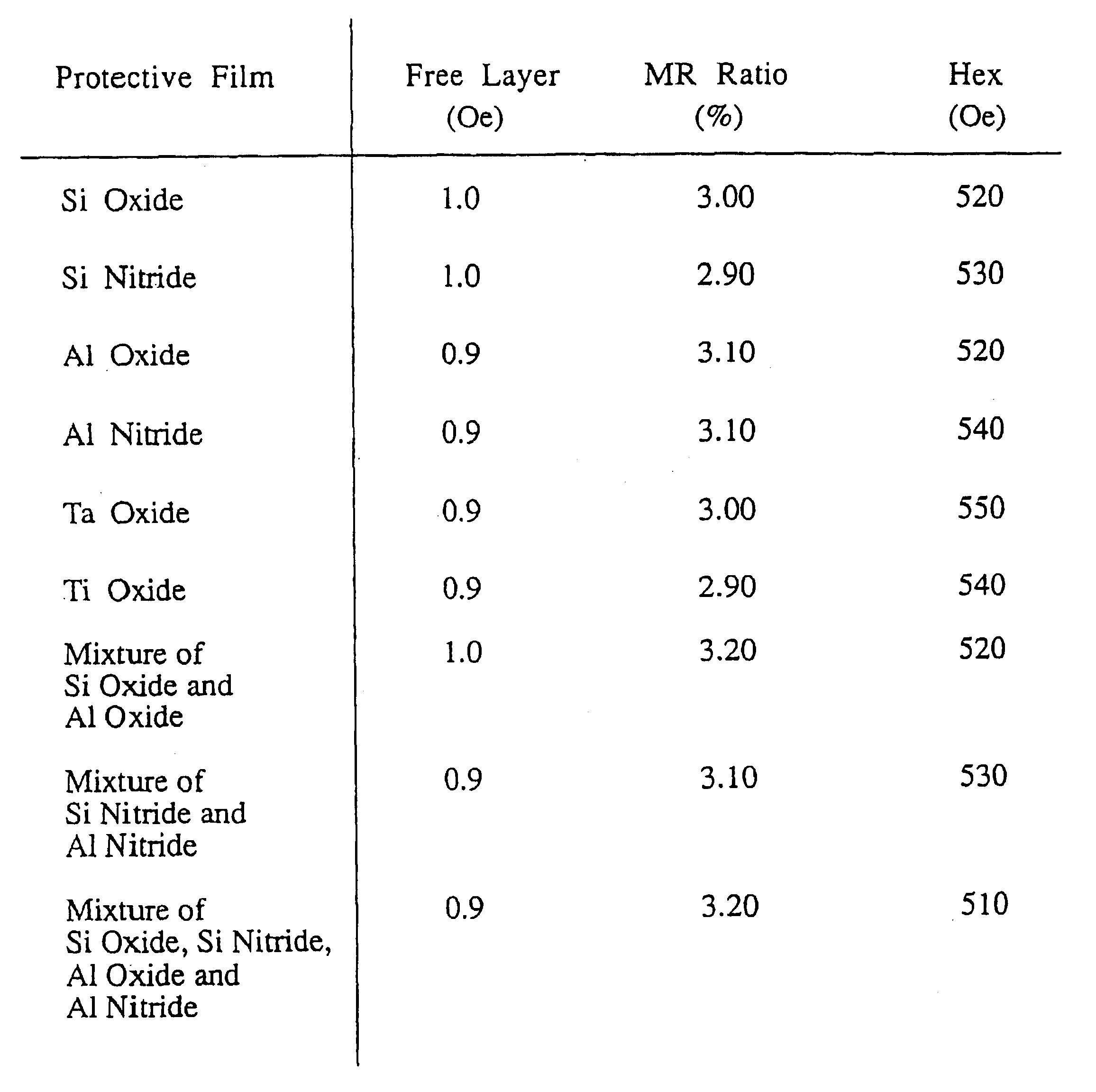
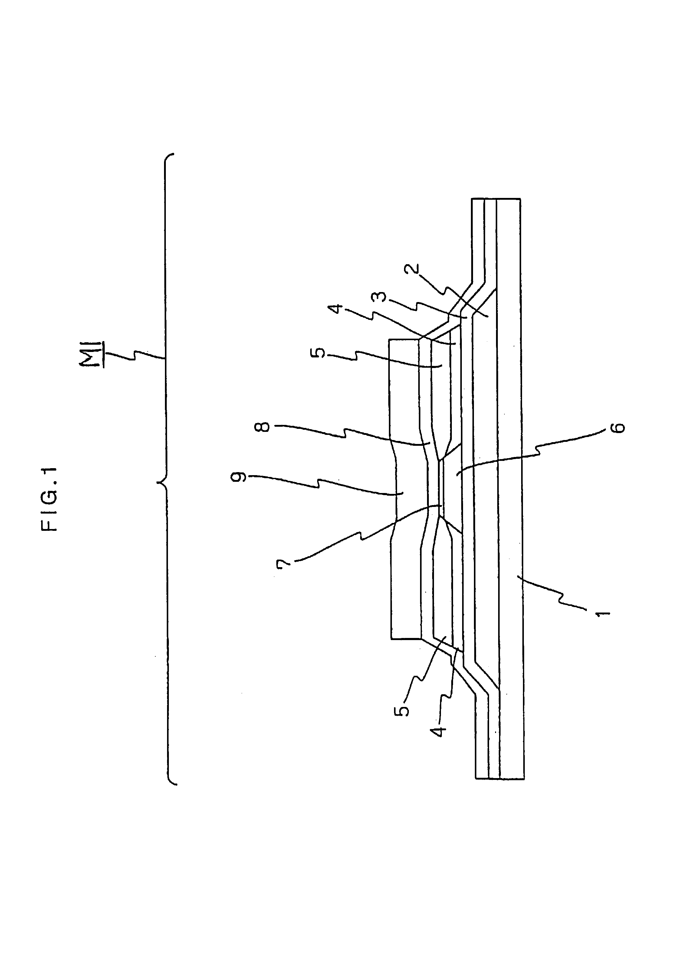
[0054]For a shielded type magnetoresistance effect sensor according to the present invention, the construction shown in FIG. 1 and FIG. 2 may be employed.

[0055]In the magnetoresistance effect sensor M1 of FIG. 1, a lower shielding layer 2, a lower gap layer 3 and a magnetoresistance effect device 6 are laminated onto a substrate 1. A gap-defining insulating layer 7 may be laminated on top of these. Lower shielding layer 2 is usually patterned to the appropriate size by a photoresist (PR) step. Magnetoresistance effect device 6 is patterned to the appropriate size and shape by a photoresist (PR) step and a vertical bias layer 4 and lower electrode layer 5 are laminated in sequence so as to join at their edges. Upper gap layer 8 and upper shielding layer 9 are laminated in sequence on top of these.

[0056]In the magnetoresistance effect sensor M2 of FIG. 2, a lower shielding layer 12, a lower gap layer 13 and a magnetoresistance effect device 16 are laminated onto a substrate 11. Lower ...


PUM

PropertyMeasurementUnit
thicknessaaaaaaaaaa
thicknessaaaaaaaaaa
atomic number ratioaaaaaaaaaa

Abstract

A magnetoresistance effect device having a basic structure wherein a multi-layer film comprising a unit of magnetic layer/non-magnetic layer/magnetic layer/antiferromagnetic layer, or antiferromagnetic layer/magnetic layer/non-magnetic layer/magnetic layer is formed with a protective film on a surface of the magnetoresistance effect device employing one of a metal, oxide material, nitride material, a mixture of oxide and nitride material, a double-layer film of metal/oxide, a double-layer film of metal/nitride, or a double-layer film of metal/(mixture of oxide and nitride) of film thickness between 2 nm and 7 nm.

Description

[0001]This application is a continuation of application Ser. No. 09 / 075,832, filed on May 12, 1998, now abandoned the entire contents of which are hereby incorporated by reference.BACKGROUND OF THE INVENTION[0002]1. Field of the Invention[0003]The present invention relates to a magnetoresistance effect device for reading an information signal recorded on a magnetic storage medium using a magnetoresistance effect sensor, and a magnetoresistance detection system and magnetic storage system.[0004]2. Description of the Related Art[0005]As prior art there is known a magnetoresistance (MR) sensor or a magnetic reading converter called an MR head. This has the characteristic feature that it can read data from the surface of a magnetic recording medium with high linear density. An MR sensor detects a magnetic field signal by means of resistance change as a function of intensity and direction of magnetic flux sensed by a reading device. Such a prior art MR sensor operates in accordance with ...

Claims


Application Information

Patent Timeline
Patent Type & Authority Patents(United States)
IPC IPC(8): G11B5/39G01R33/09G11B5/00G11B5/012H01F10/08H01F10/32H01L43/08
CPCB82Y10/00B82Y25/00G01R33/093G11B5/3967G11B5/012G11B5/3903G11B5/00G11B5/3906G11B2005/3996
Inventor HAYASHI, KAZUHIKO
Owner TDK CORPARATION
Why Eureka
Try Eureka