Lateral double diffused MOSFET device

a technology of mosfet and metal oxide, which is applied in the direction of semiconductor devices, basic electric elements, electrical equipment, etc., can solve the problems of difficulty in forming deep trenches, semiconductor devices that take trouble and time to manufacture, and thick film soi substrates b>102/b> having a box layer b>104/b> with a layer thickness of no less than 4 m, etc., to achieve the effect of small layer thickness of semiconductor

Active Publication Date: 2016-03-29
ROHM CO LTD
View PDF24 Cites 1 Cited by
  • Summary
  • Abstract
  • Description
  • Claims
  • Application Information

AI Technical Summary

Benefits of technology

[0013]An object of the present invention is to provide a semiconductor device that enables a layer thickness of a semiconductor layer to be small without lowering a withstand voltage of an element.
[0016]By forming the first conductive type region, the depletion layer can be suppressed from extending toward the drain region. Thus, the layer thickness of the semiconductor layer can be small without lowering the withstand voltage of the element formed in the element forming region. Consequently, the deep trench can be formed readily, and the trouble and time required to manufacture the semiconductor device can be reduced.

Problems solved by technology

When the layer thickness of the SOI layer 105 is large, it is difficult to form the deep trench 106 and the semiconductor device takes trouble and time to manufacture.
However, a thick film SOI substrate 102 having a BOX layer 104 with a layer thickness of no less than 4 μm cannot be manufactured by current arts.

Method used


Image

  • Lateral double diffused MOSFET device
  • Lateral double diffused MOSFET device
  • Lateral double diffused MOSFET device

Examples


first embodiment

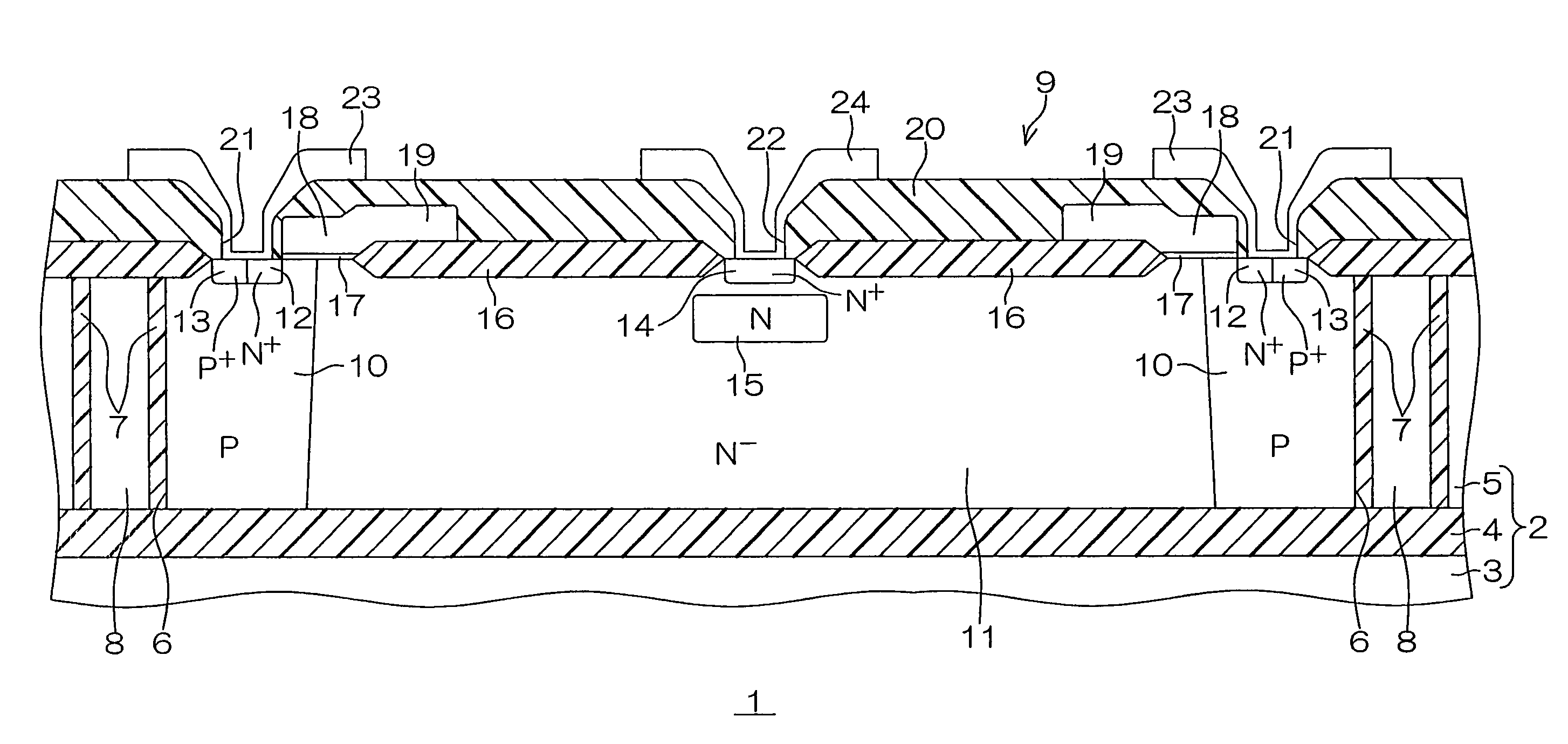
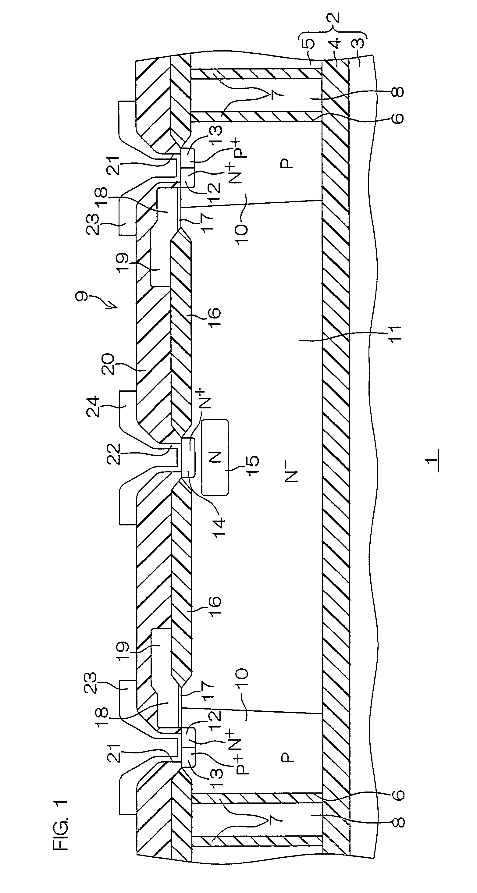
[0036]FIG. 1 is a schematic sectional view of a structure of a semiconductor device according to the present invention.

[0037]The semiconductor device 1 includes a thick film SOI substrate 2. The thick film SOI substrate 2 has a structure where an N−-type SOI layer 5 made of Si is laminated on a silicon substrate 3 via a BOX layer 4 as an insulating layer made of SiO2. A layer thickness of the BOX layer 4 is, for example, 1.5 μm and the layer thickness of the SOI layer 5 is, for example, 30 μm. An N-type impurity concentration of the SOI layer 5 is, for example, 3.5×10¹⁴ / cm3.

[0038]An annular deep trench 6 is penetratingly formed in the layer thickness direction in the SOI layer 5 as a semiconductor layer. That is, the annular deep trench 6 having a depth reaching from the top surface of the SOI layer 5 to the BOX layer 4 is formed in the SOI layer 5. An inner side surface of the deep trench 6 is covered with a silicon oxide film 7. An inner side of the silicon oxide film 7 is complet...

second embodiment

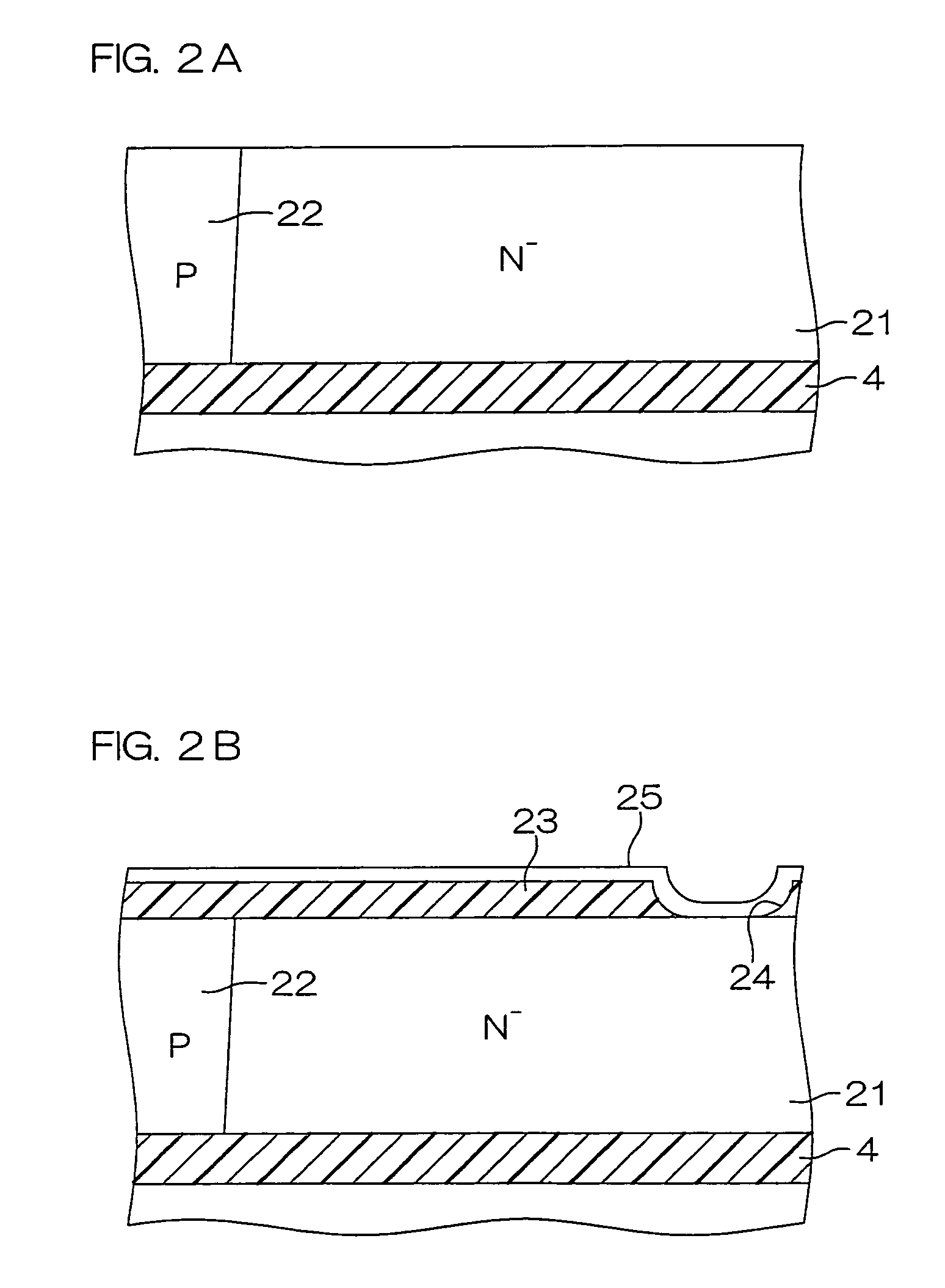
[0057]FIG. 4 is a schematic sectional view of a structure of a semiconductor device according to the present invention. In FIG. 4, portions equivalent to respective portions shown in FIG. 1 are provided with the same reference symbols as the respective portions. In regard to the structure shown in FIG. 4, differences with respect to the structure shown in FIG. 1 shall mainly be described below, and description of portions equivalent to the respective portions shown in FIG. 1 shall be omitted.

[0058]With the semiconductor device 1 shown in FIG. 1, the N-type region 15 is formed spaced apart from and at the BOX layer 4 side of the drain region 14. Meanwhile, with the semiconductor device 41 shown in FIG. 4, in the drift region 11, an N-type region 42 having an N-type impurity concentration higher than the N-type impurity concentration of the SOI layer 5 and lower than the N-type impurity concentration of the drain region 14 is formed adjacent to and at the BOX layer 4 side of the drain...


PUM


Abstract

A semiconductor device according to the present invention includes: an insulating layer; a semiconductor layer of a first conductive type laminated on the insulating layer; an annular deep trench having a thickness reaching the insulating layer from a top surface of the semiconductor layer; a body region of a second conductive type formed across an entire thickness of the semiconductor layer along a side surface of the deep trench in an element forming region surrounded by the deep trench; a drift region of the first conductive type constituted of a remainder region besides the body region in the element forming region; a source region of the first conductive type formed in a top layer portion of the body region; a drain region of the first conductive type formed in a top layer portion of the drift region; and a first conductive type region formed in the drift region, having a deepest portion reaching a position deeper than the drain region, and having a first conductive type impurity concentration higher than the first conductive type impurity concentration of the semiconductor layer and lower than the first conductive type impurity concentration of the drain region.

Description

BACKGROUND OF THE INVENTION[0001]1. Field of the Invention[0002]The present invention relates to a semiconductor device including an LDMOSFET (Lateral Double Diffused Metal Oxide Semiconductor Field Effect Transistor).[0003]2. Description of Related Art[0004]Among semiconductor devices including an LDMOSFET, there is a configuration employing a thick film SOI (Silicon On Insulator) substrate as a base to increase withstand voltage of the LDMOSFET.[0005]FIG. 6 is a schematic sectional view of a semiconductor device including an LDMOSFET of high withstand voltage.[0006]A thick film SOI substrate 102 forming a base of the semiconductor device 101 has a structure where an SOI layer 105 made of Si (silicon) is laminated on a silicon substrate 103 via a BOX (buried oxide) layer 104 made of SiO2 (silicon dioxide).[0007]An annular deep trench 106 is formed by digging in from a top surface of the SOI layer 105. A deepest portion of the deep trench 106 reaches the BOX layer 104. An interior o...

Claims


Application Information

Patent Timeline
Patent Type & Authority Patents(United States)
IPC IPC(8): H01L29/76H01L29/78H01L29/08H01L29/66H01L29/423
CPCH01L29/7824H01L29/0878H01L29/66681H01L29/42368H01L29/1083H01L29/1095H01L29/402
Inventor IZUMI, NAOKISADA, TOMOYASU
Owner ROHM CO LTD
Why Eureka
Try Eureka