Photoelectric conversion device, imaging device, method for manufacturing imaging device, and imaging apparatus

a technology of photoelectric conversion and imaging device, which is applied in thermoelectric devices, solid-state devices, and nano-informatics. it can solve the problems of large dark current, inability to consider how to suppress a free carrier, and inability to effectively suppress the dark current by the free carrier upwelled in the photoelectric conversion layer. it can reduce the effect of dark curren

Active Publication Date: 2013-12-24
FUJIFILM CORP
View PDF14 Cites 2 Cited by
  • Summary
  • Abstract
  • Description
  • Claims
  • Application Information

AI Technical Summary

Benefits of technology

[0029]It may be considered that the dark current derived from the free carrier generated in the photoelectric conversion layer is expressed by a product of a carrier amount (electron spin number in the invention), a mobility (resistance of the film) of the photoelectric conversion layer and an electric field intensity to be impressed to the photoelectric conversion layer. For that reason, it may be considered that the effect of the invention is revealed especially conspicuously in a state of a high mobility of the photoelectric conversion layer (in a state of a low resistance of the film) or in a state of a high impressed electric field intensity. In order to conspicuously reveal the effect of the invention, the mobility of the photoelectric conversion layer is preferably 1×10⁻⁶ cm2 / Vs or more, more preferably 1×10⁻⁵ cm2 / Vs or more, and still more preferably 5×10⁻⁴ cm2 / Vs or more.
[0030]As a constitution capable of realizing a photoelectric conversion layer having the foregoing mobility, a mixed layer of a p-type material and an n-type material is preferable. When the mixed layer of a p-type material and an n-type material is formed, and a path resulting from connection of p-type materials and a path resulting from connection of n-type materials are formed, the hole in the layer is transported into the path formed by the p-type materials, and the electron in the layer is transported into the path formed by the n-type materials. This is because the p-type material has a high hole mobility, and the n-type material has a high electron mobility. so that both the electron and the hole are rapidly transported in the foregoing layer, the layer resistance becomes small, and the contribution of the carrier amount in the photoelectric conversion layer (electron spin number in the invention) to the dark current becomes large.
[0031]That is, in the case of the single p-type material or the single n-type material, either one of hole transport properties or electron transport properties are high, with the remainder being low, and therefore, there is a tendency that the resistance of the layer is high, and the dark current value is relatively low. However, in that case, since optical signals are hardly transported, and a photoelectric conversion efficiency (amount of charges capable of being collected) decreases, there may be the case where the S / N is lowered. As described later, by taking the mixed layer of a p-type material and an n-type material, the exciton dissociation interface number in the layer increases, thereby enabling the sensitivity to be increased. However, in that case, a carrier due to thermal excitation is generated at the interface, resulting in an increase in the dark current. For that reason, it is important to minimize the electron spin number (carrier amount) in the photoelectric conversion layer as specified in the invention.
[0032]In the invention, the electron spin number per cm3 of the photoelectric conversion layer at room temperature (25° C.) is preferably not more than 1.0×10¹⁵, more preferably not more than 1×10¹⁴, and still more preferably not more than 8×10¹³.
[0033]In order to suppress the free carrier to be generated due to impurities or the like, with respect to the material per se to be used for the photoelectric conversion layer, when a risk of incorporation of a free carrier generation source such as impurities contained in the material into the photoelectric conversion layer is also taken into consideration, it is preferable that the own electron spin number of the material (the value identified in the state of the material as it is but not in the state where the material has been subjected to thin film fabrication) is small, and it may be considered that the electron spin number is preferably not more than 1.0×10¹⁵ / cm3, more preferably not more than 1.0×10¹⁴ / cm3, further preferably 8.0×10¹³ / cm3.
[0034]However, as described previously, the own electron spin number of the material is not single-mindedly corresponding to the electron spin number in the layered state, and the electron spin number in the layered state is exactly important. Therefore, even when only the own electron spin number of the material is specified, the effects described in this specification cannot be always obtained.

Problems solved by technology

However, when a photoelectric conversion material or a bulk hetero layer which is used in a photoelectric conversion layer in organic thin film solar cells or the like is applied to an imaging device as it is, in many cases, the dark current becomes large.
However, a method for effectively suppressing the dark current by the free carrier upwelled in the photoelectric conversion layer has not been known yet.
However, all of JP-A-2009-54794, JP-A-2008-115460 and JP-A-2004-363577 show a thought that there is a correlation between a defect (dangling bond) in an inorganic material layer and an electron spin density, but they do not consider how to suppress a free carrier which will possibly become a dark current source in a photoelectric conversion layer where a dangling bond does not exist (specifically, an organic material-containing photoelectric conversion layer).

Method used


Image

  • Photoelectric conversion device, imaging device, method for manufacturing imaging device, and imaging apparatus
  • Photoelectric conversion device, imaging device, method for manufacturing imaging device, and imaging apparatus
  • Photoelectric conversion device, imaging device, method for manufacturing imaging device, and imaging apparatus

Examples


example 1

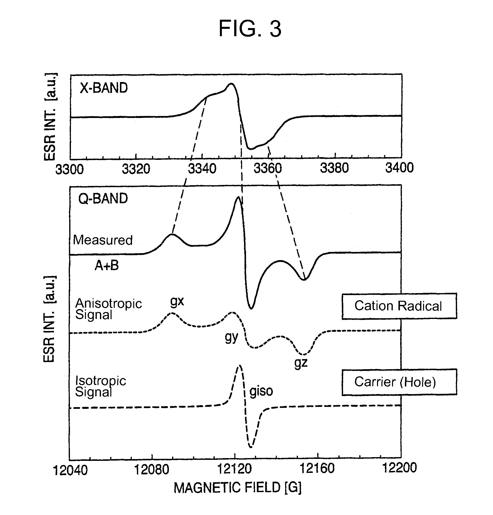
[0199]An imaging device equipped with an organic photoelectric conversion device was fabricated. However, in the imaging device, the formation of configurations above a counter electrode was omitted. The procedures are as follows.

[0200]First of all, amorphous ITO was subjected to thin film fabrication in a thickness of 30 nm on a CMOS substrate in which read-out circuits composed of a CMOS circuit and connection electrodes to be connected thereto had been formed, by a sputtering method, followed by patterning to form a pixel electrode on each of the connection electrodes. Subsequently, Compound 2 was subjected to thin film fabrication in a thickness of 100 nm on the plural pixel electrodes by a vacuum vapor deposition method, thereby forming an electron blocking layer. Subsequently, Compound 1 as a p-type organic material and fullerene (C60) as an n-type organic material were subjected to thin film fabrication in a thickness as reduced into a single layer of 100 nm and 200 nm, respe...

example 2

[0202]An imaging device was fabricated in the same manner as in Example 1, except that Compound 1 was changed to Compound 3, and the electron spin number of the photoelectric conversion layer was identified in the same manner as in Example 1.

example 3

[0203]An imaging device was fabricated in the same manner as in Example 1, except that Compound 1 was changed to Compound 4, and the electron spin number of the photoelectric conversion layer was identified in the same manner as in Example 1.


PUM


Abstract

An organic photoelectric conversion device having: a first electrode; a second electrode opposing to the first electrode; and an organic material-containing photoelectric conversion layer provided between the first electrode and the second electrode, wherein an electron spin number of the photoelectric conversion layer is not more than 1.0×10¹⁵ / cm3.

Description

CROSS-REFERENCE TO RELATED APPLICATION(S)[0001]The present application claims priority from Japanese Patent Application No. 2010-041125 filed on Feb. 25, 2010, the entire content of which is incorporated herein by reference.BACKGROUND[0002]1. Field[0003]The present invention relates to a photoelectric conversion device, an imaging device, a method for manufacturing an imaging device and an imaging apparatus.[0004]2. Description of the Related Art[0005]JP-A-2007-88033 discloses an organic photoelectric conversion device having a pair of electrodes and an organic compound-containing photoelectric conversion layer provided between the electrodes. The photoelectric conversion layer as referred to herein means a layer which receives light to generate a charge corresponding to the amount of received light. Also, JP-A-2009-147147 discloses an imaging device using such an organic photoelectric conversion device. Since performances such as high sensitivity and low dark current are required i...

Claims


Application Information

Patent Timeline
Patent Type & Authority Patents(United States)
IPC IPC(8): H01L31/04
CPCB82Y10/00H01L27/307H01L51/0059H01L51/0047H10K39/32H10K85/215H10K85/631
Inventor MITSUI, TETSUROKOMIYAMA, TAKASHISUGIYAMA, TAKURO
Owner FUJIFILM CORP
Why Eureka
Try Eureka