Method and apparatus for a flash memory device comprising a source local interconnect

a source local interconnect and flash memory technology, applied in the direction of semiconductor devices, electrical apparatus, transistors, etc., can solve the problems of increasing the electrical resistance of the source diffusion region beyond a desirable level, and increasing the resistance of the device. , to achieve the effect of reducing the spacing and more scaleable devices

Inactive Publication Date: 2005-04-19
MICRON TECH INC
View PDF14 Cites 2 Cited by
  • Summary
  • Abstract
  • Description
  • Claims
  • Application Information

AI Technical Summary

Benefits of technology

[0011]The present invention provides a new method for forming a semiconductor device, and an inventive semiconductor device resulting from the method, which, among other advantages, allows for a more scaleable device than is found with flash memory devices having diffused sources. The inventive method and device further allows for minimal spacing between a local interconnect and adjacent transistor features.

Problems solved by technology

One obstacle to decreasing the transistor size is that if the cross-sectional area of the source region 12 becomes too small the electrical resistance of the source diffusion region increases beyond a desirable level and the device may become unreliable.
The undesirable increase in resistance is exacerbated by the relatively extreme length of the diffusion region which functions as a source region for all transistors within a column.
One problem with providing a heavily doped source region is that the dopants tend to diffuse away from the source region, especially with high-temperature processing of subsequent manufacturing steps.
This decrease in channel length can produce problems known as “short channel effects” such as a transistor with a lowered threshold voltage, which itself can produce an unreliable device.

Method used


Image

  • Method and apparatus for a flash memory device comprising a source local interconnect
  • Method and apparatus for a flash memory device comprising a source local interconnect
  • Method and apparatus for a flash memory device comprising a source local interconnect

Examples


first embodiment

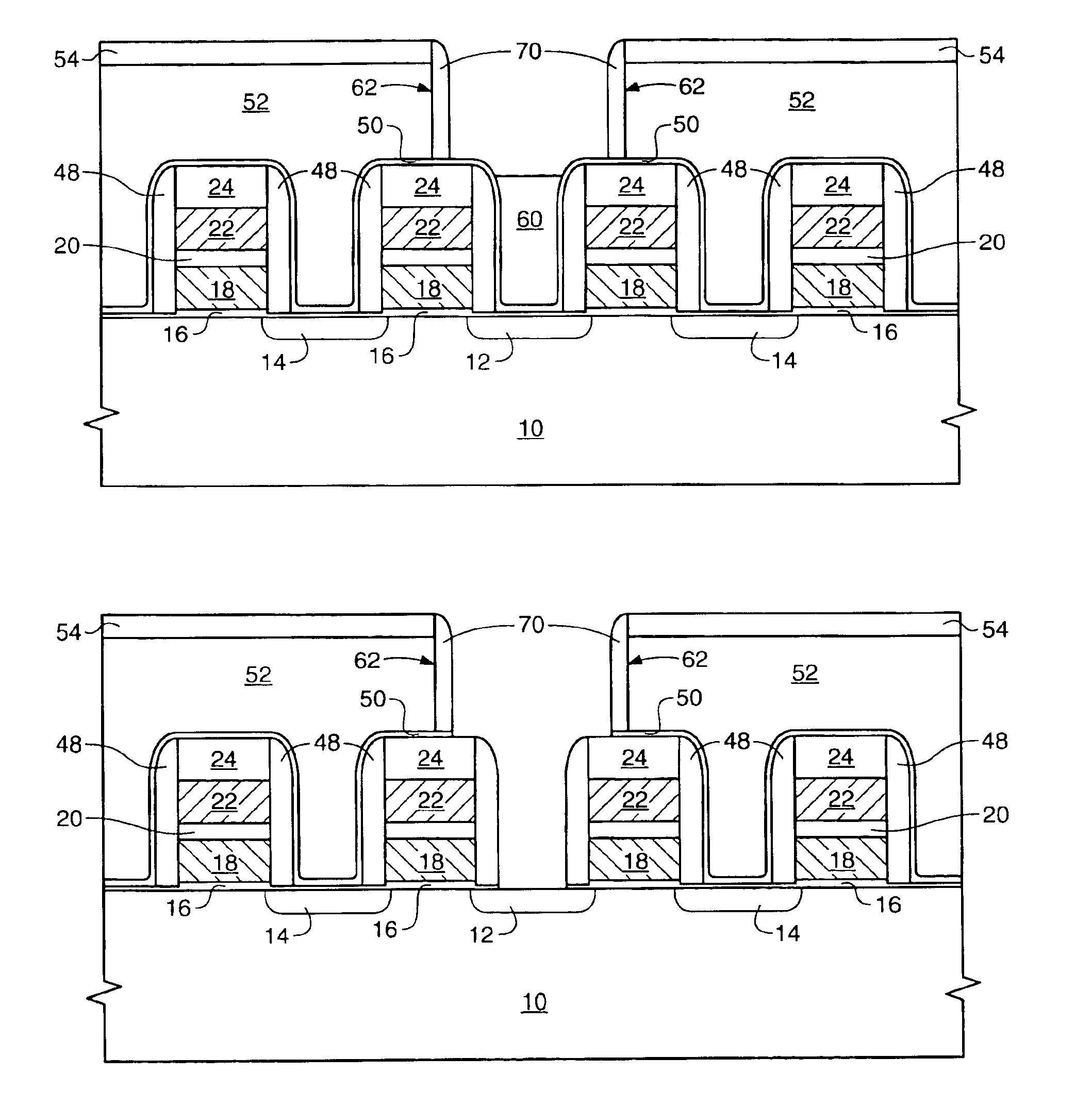
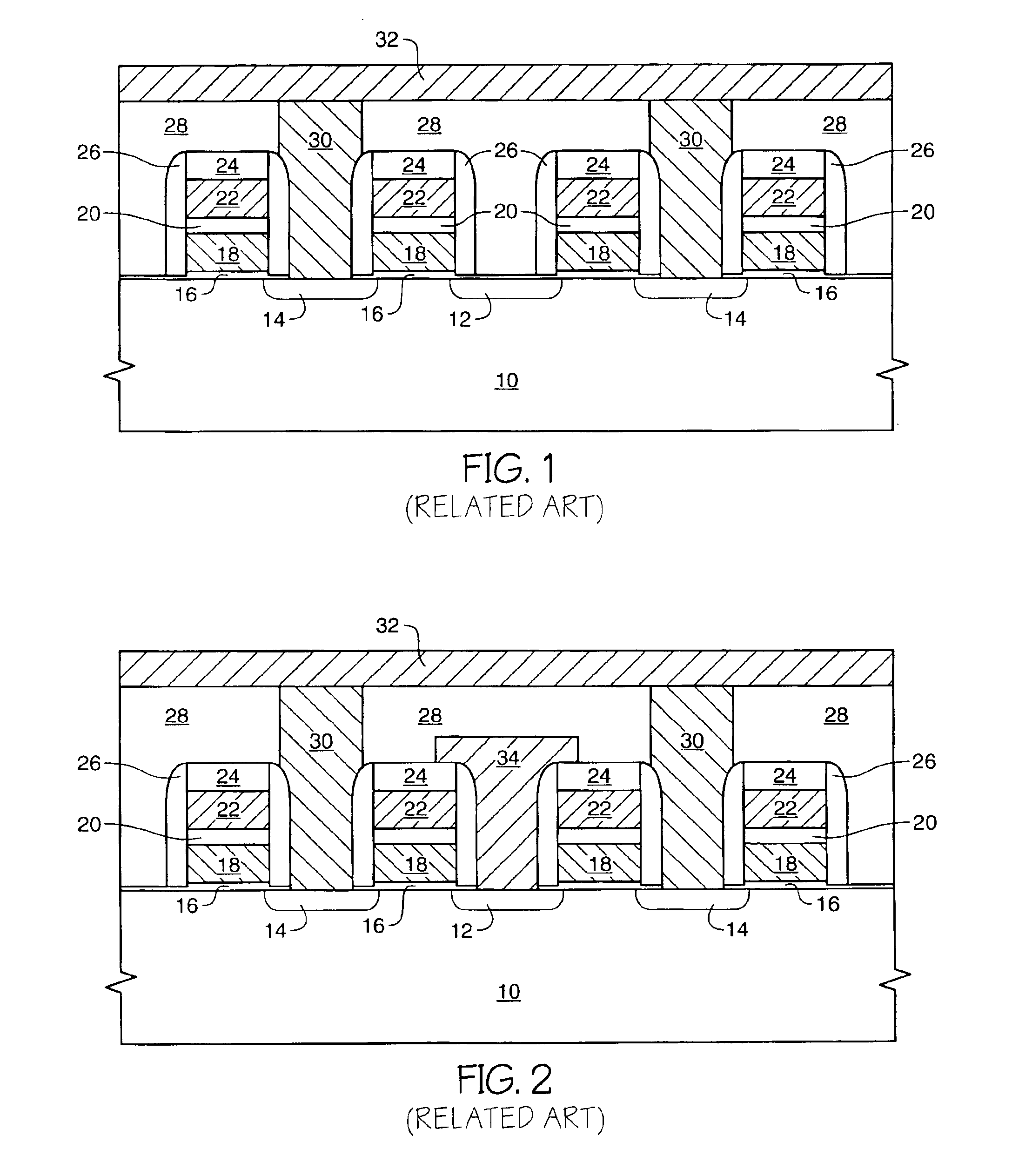
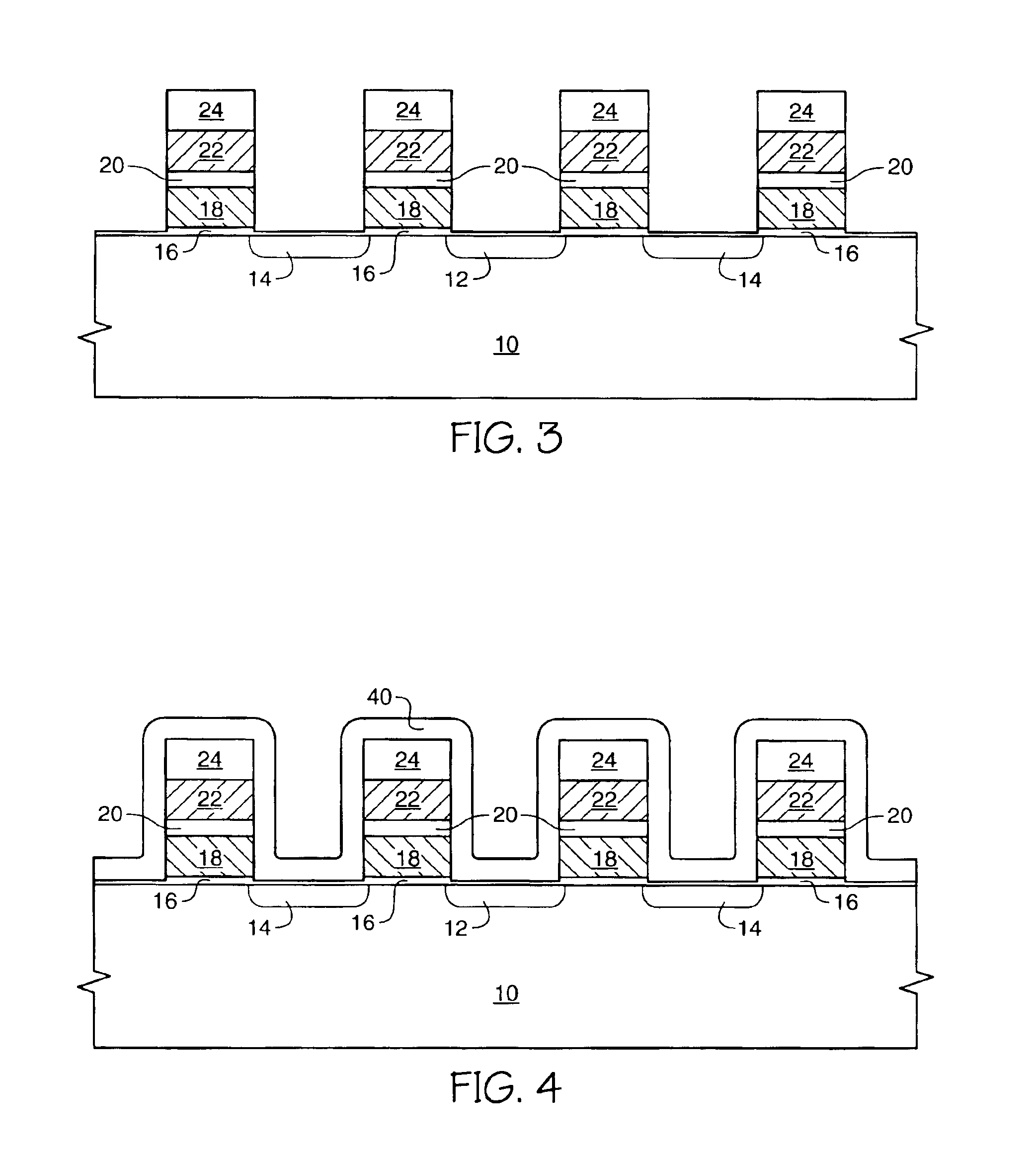
[0023]an inventive method for providing a flash memory device comprising a source local interconnect is depicted in FIGS. 3-12. The structure of FIG. 3, or a similar structure, is formed to comprise the following: a semiconductor wafer 10, implanted transistor source 12 and drain 14 diffusion regions, gate oxide 16, floating gates 18, capacitor dielectric 20, control gates 22, and a capping layer 24, for example comprising silicon nitride (Si3N4). While four transistor stacks comprising layers 16-24 are depicted, it is conventional that a transistor array comprising several million transistors will be located over the surface of wafer 10.

[0024]The source regions 12 can comprise an arsenic-doped or phosphorous-doped well implanted in the wafer to an implant level of between about 1E13 to about 1E15 atoms / cm2. This is different from conventional flash devices which have a source implant level of greater than 1E15 up to about 1E16 atoms / cm2. The lighter doping concentration of the inve...

second embodiment

[0035]the inventive method is depicted in FIGS. 13-16. FIG. 13 depicts the following device structures: a semiconductor wafer 10, implanted transistor source 12 and drain 14 diffusion regions, gate oxide 16, a floating gate 18, capacitor dielectric 20, a control gate 22, and a capping layer 24, for example comprising silicon nitride (Si3N4). The source regions 12 can comprise an arsenic-doped or phosphorous-doped well implanted in the wafer to an implant dose of between about 1E13 to about 1E15 atoms / cm2. As stated in reference to the prior embodiment, this is different from conventional flash devices which have a source implant level of greater than 1E15 up to about 1E16 atoms / cm2. The lighter implant dose of the inventive source region allows the distance between flash cell source and drain to be decreased. This decrease in spacing between the source and drain allowed by this embodiment of the present invention results, in part, from the reduction of the number of implanted atoms ...


PUM


Abstract

A method for forming a flash memory device having a local interconnect connecting source regions of a plurality of transistors within a sector allows for a highly-selective wet etch of a dielectric region overlying the source region. An embodiment of the method comprises the use of an etch-resistant layer covering various features such as any gate oxide remaining over the source region, spacers along sidewalls of the transistor stacks, and a capping layer of the transistor. An in-process semiconductor device resulting from the inventive method is also disclosed.

Description

[0001]This is a division of U.S. Ser. No. 10 / 232,221 filed Aug. 29, 2002 and issued Sep. 23, 2003 as U.S. Pat. No. 6,624,024.FIELD OF THE INVENTION[0002]This invention relates to the field of semiconductor manufacture and, more particularly, to a method and structure for a source local interconnect for a flash memory device.BACKGROUND OF THE INVENTION[0003]Floating gate memory devices such as flash memories include an array of electrically-programmable and electrically-erasable memory cells. Typically, each memory cell comprises a single n-channel metal oxide semiconductor (NMOS) transistor including a floating gate interposed between a control (input) gate and a channel. A layer of high-quality tunnel oxide used as gate oxide separates the transistor channel and the floating gate, and an oxide-nitride-oxide (ONO) dielectric stack separates the floating gate from the control gate. The ONO stack typically comprises a layer of silicon nitride (Si3N4) interposed between underlying and ...

Claims


Application Information

Patent Timeline
Patent Type & Authority Patents(United States)
IPC IPC(8): H01L29/76H01L21/70H01L29/66H01L21/8247H01L29/788H01L31/062H01L31/06H01L21/336H01L21/60H01L21/768H01L27/082H01L27/102H01L27/115H01L29/70H01L31/11
CPCH01L21/76895H01L21/76897H01L21/76831H01L27/11521H01L27/115H10B69/00H10B41/30
Inventor PRALL, KIRK D.CHEN, CHUN
Owner MICRON TECH INC
Why Eureka
Try Eureka