Method and structure for a self-aligned silicided word line and polysilicon plug during the formation of a semiconductor device

a technology of polysilicon plug and silicon silicide, which is applied in the direction of semiconductor devices, basic electric elements, electrical equipment, etc., can solve the problems of increasing junction leakage, increasing junction leakage, and increasing the difficulty of titanium silicide scaling, so as to reduce the size of features, reduce the difficulty of scaling, and reduce the effect of problems

Active Publication Date: 2005-01-13
MICRON TECH INC
View PDF17 Cites 15 Cited by
  • Summary
  • Abstract
  • Description
  • Claims
  • Application Information

AI Technical Summary

Benefits of technology

[0009] The present invention provides a new method and structure which, among other advantages, reduces problems associated with the manufacture of semiconductor devices, particularly problems resulting from the formation of a mask during a process which provides a silicide layer over various polysilicon features. An embodiment of the invention further provides an advantage of the formation of a silicide layer which is more scaleable with decreasing features sizes than previous silicide layers.

Problems solved by technology

As the sizes of the plugs and line widths decrease with improved manufacturing technology, the doped polysilicon structure may provide insufficient conductance and excessive resistance.
While the silicide layer interposed between the silicon wafer and the polysilicon plug provides decreased resistance and increased conductance, it can also provide a path for leakage between an adjacent transistor channel region and an active area, thereby increasing junction leakage.
Further, titanium silicide becomes more difficult to scale as feature sizes decrease.

Method used


Image

  • Method and structure for a self-aligned silicided word line and polysilicon plug during the formation of a semiconductor device
  • Method and structure for a self-aligned silicided word line and polysilicon plug during the formation of a semiconductor device
  • Method and structure for a self-aligned silicided word line and polysilicon plug during the formation of a semiconductor device

Examples


Embodiment Construction

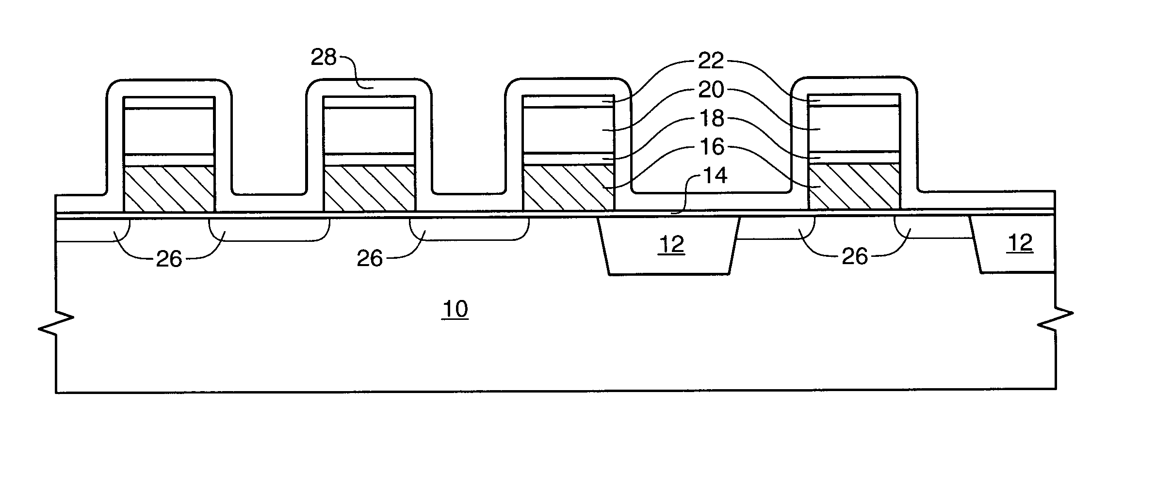
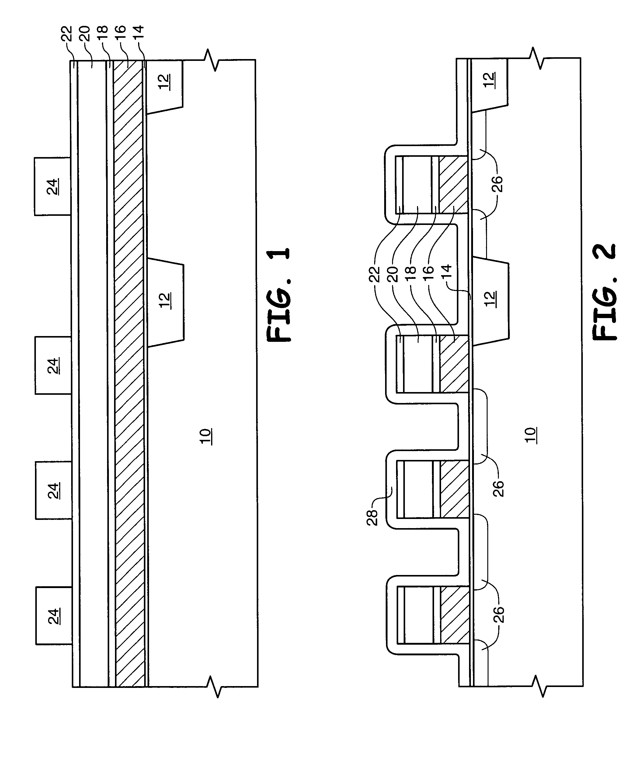
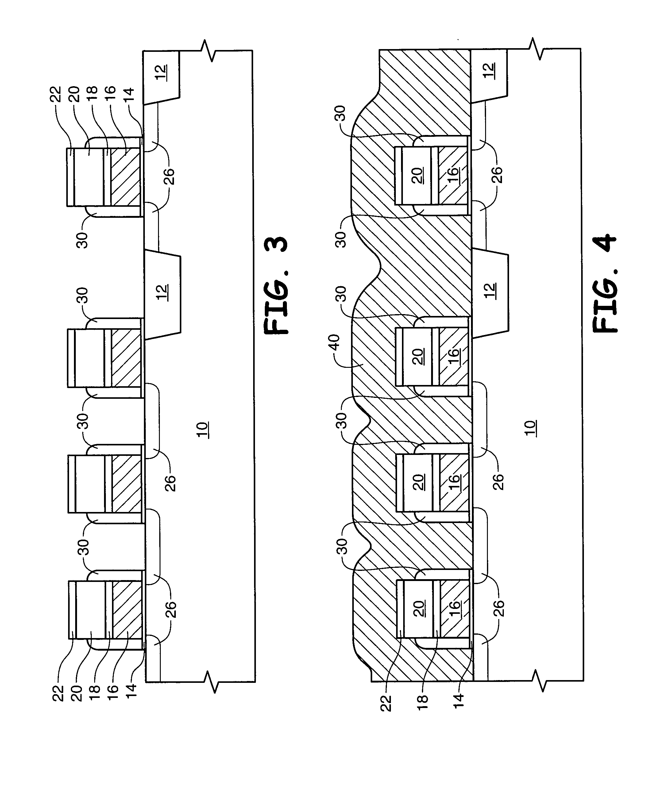
[0017] The term “wafer” is to be understood as a semiconductor-based material including silicon, silicon-on-insulator (SOI) or silicon-on-sapphire (SOS) technology, doped and undoped semiconductors, epitaxial layers of silicon supported by a base semiconductor foundation, and other semiconductor structures. Furthermore, when reference is made to a “wafer” in the following description, previous process steps may have been performed to provide regions or junctions in or over the base semiconductor structure or foundation. Additionally, when reference is made to a “substrate assembly” in the following description, the substrate assembly may include a wafer with layers including dielectrics and conductors, and features such as transistors, formed thereover, depending on the particular stage of processing. In addition, the semiconductor need not be silicon-based, but could be based on silicon-germanium, silicon-on-insulator, silicon-on-sapphire, germanium, or gallium arsenide, among othe...


PUM


Abstract

A method used to form a semiconductor device provides a silicide layer on a plurality of transistor word lines and on a plurality of conductive plugs. In one embodiment, the word lines, one or more sacrificial dielectric layers on the word lines, conductive plugs, and a conductive enhancement layer are formed through the use of a single mask. An in-process semiconductor device which can be formed using one embodiment of the inventive method is also described.

Description

FIELD OF THE INVENTION [0001] This invention relates to the field of semiconductor manufacture, and more particularly to a process for forming self-aligned conductive structures having enhanced conductivity through an enhancement layer, and an inventive structure resulting from the process. BACKGROUND OF THE INVENTION [0002] Structures such as polycrystalline silicon (polysilicon) plugs, interconnects, and transistor gates are commonly formed during the manufacture of semiconductor devices such as microprocessors, memory devices, and logic devices. To manufacture a plug, for example, a masked dielectric layer is formed over an underlying substrate assembly and an etch is completed to form a hole in the dielectric which exposes the underlying structure in the area where contact is to be made. A blanket polysilicon layer is deposited over the dielectric layer which fills the hole in the dielectric layer and contacts the underlying structure. The polysilicon is then removed from a plan...

Claims


Application Information

Patent Timeline
Patent Type & Authority Applications(United States)
IPC IPC(8): H01L21/28H01L21/285H01L21/336H01L21/60H01L21/768H01L21/8239H01L21/8242H01L29/49
CPCH01L21/28052H01L21/76889H01L21/76897H01L27/1052H01L29/4933H01L29/66545H01L27/10873H10B99/00H10B12/05
Inventor FISHBURN, FREDRICK D.MCDANIEL, TERRENCE B.LANE, RICHARD H.
Owner MICRON TECH INC
Why Eureka
Try Eureka