Nanoscale field-emission device and method of fabrication

Active Publication Date: 2019-07-30
CALIFORNIA INST OF TECH
View PDF2 Cites 0 Cited by
  • Summary
  • Abstract
  • Description
  • Claims
  • Application Information

AI Technical Summary

Benefits of technology

The present invention is about a new field-emission device that can operate without causing damage to the electrodes through thermionic emission or impact ionization. The device employs small gaps between the electrodes, which allows for the application of low voltage to induce electron emission. This low energy level of the emitted electrons prevents damage to the gas molecules in the gap. Compared to previous devices that use thermionic emission, the present invention experiences less degradation and failure due to high-temperature heating. In some embodiments, the gap is 200 nm or less, making operation at atmospheric pressure a possibility. The diode described in the patent text has an emitter electrode and a collector electrode with a gap of 22 nm between them. The electrodes are made of single-crystal silicon doped with phosphorous. The device is formed by etching the active layer of a silicon-on-insulator wafer and providing electrical contacts to each electrode, with some or all of the exposed regions of the buried oxide layer of the wafer being etched back to increase the oxide path between the electrodes and reduce leakage current.

Problems solved by technology

Since the applied voltage is low, the energy of the emitted electrons is below the ionization potential of the gas or gasses residing in the gap, thereby mitigating impact ionization of the gas molecules by the emitted electrons and the resultant electrode damage.

Method used


Image

  • Nanoscale field-emission device and method of fabrication
  • Nanoscale field-emission device and method of fabrication
  • Nanoscale field-emission device and method of fabrication

Examples


Embodiment Construction

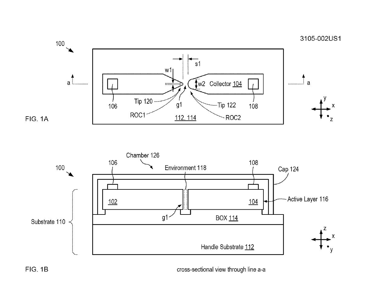
[0041]FIGS. 1A-B depict schematic drawings of top and cross-sectional views, respectively, of a field-emission device in accordance with an illustrative embodiment of the present invention. Device 100 is an edge-emitting, two-terminal field-emission device having an asymmetric current-voltage characteristic, which enables the device to operate in diode-like fashion. Device 100 includes emitter 102 and collector 104. The cross-sectional view of device 100 depicted in FIG. 1B is taken though line a-a as shown in FIG. 1A.

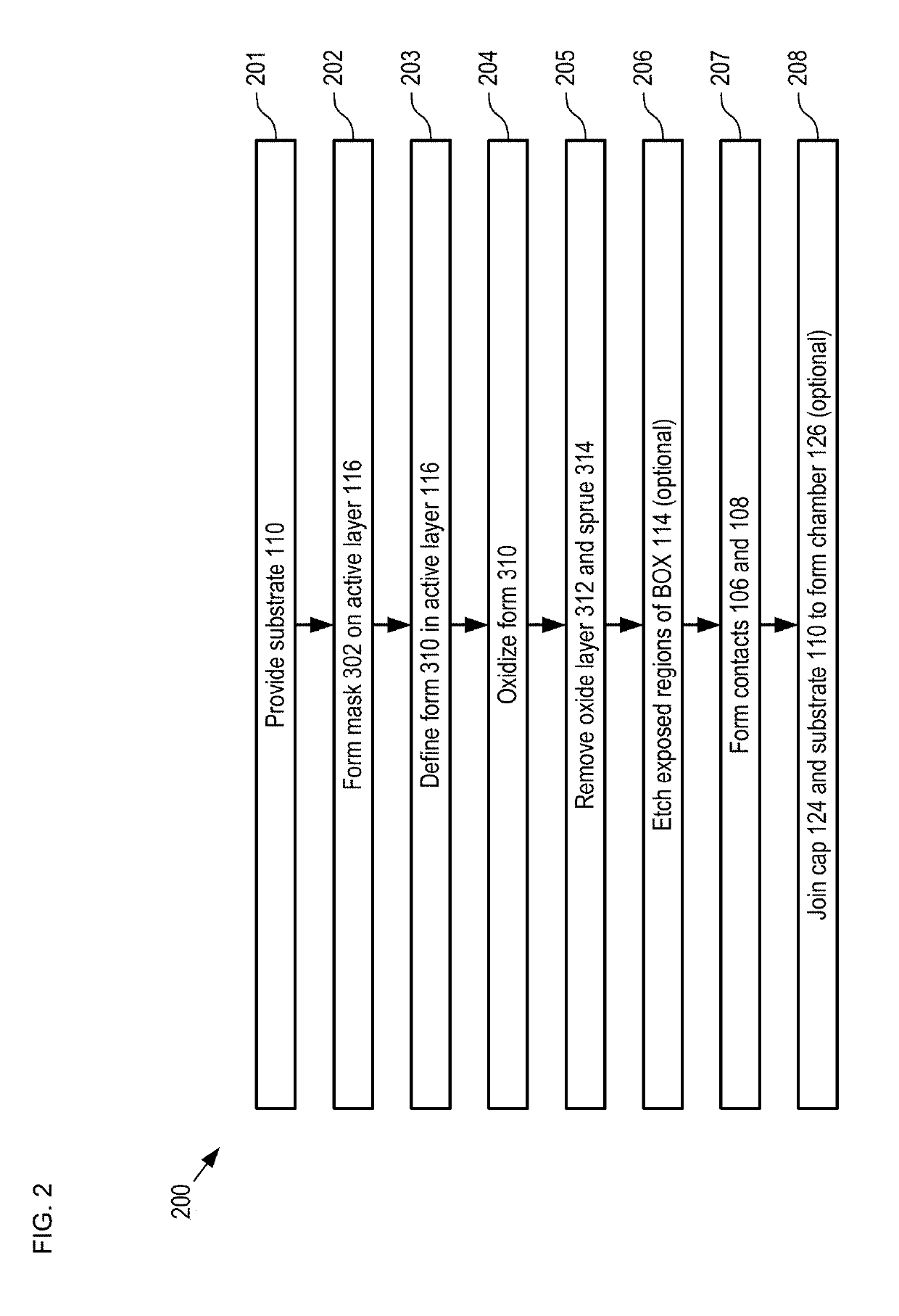
[0042]FIG. 2 depicts operations of a method for forming a field-emission device in accordance with the illustrative embodiment. Method 200 begins with operation 201, wherein substrate 110 is provided. Method 200 is described herein with continuing reference to FIGS. 1A-B, as well as reference to FIGS. 3A-D.

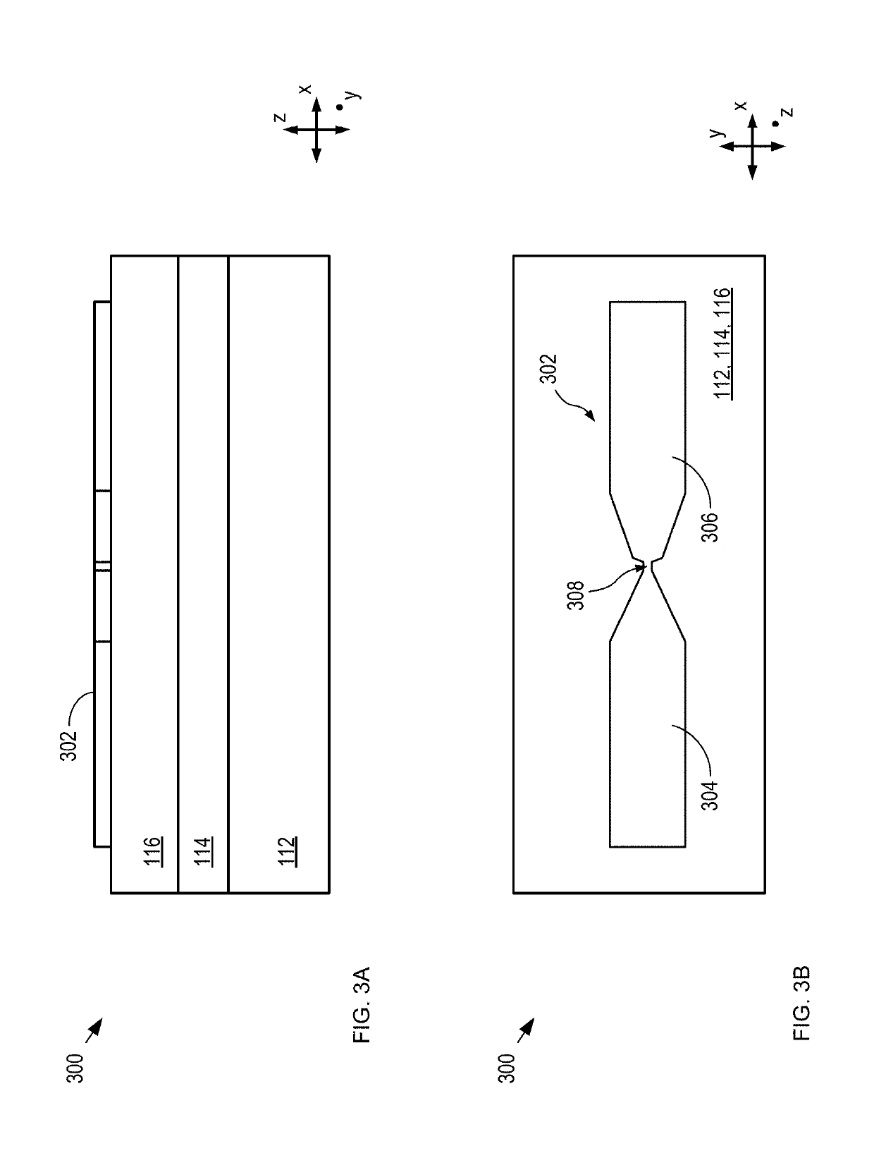
[0043]FIGS. 3A-E depict schematic drawings of top and cross-sectional views (though line a-a) of a nascent field-emission device at different stages of its fabricati...


PUM


Abstract

Nanoscale field-emission devices are presented, wherein the devices include at least a pair of electrodes separated by a gap through which field emission of electrons from one electrode to the other occurs. The gap is dimensioned such that only a low voltage is required to induce field emission. As a result, the emitted electrons energy that is below the ionization potential of the gas or gasses that reside within the gap. In some embodiments, the gap is small enough that the distance between the electrodes is shorter than the mean-free path of electrons in air at atmospheric pressure. As a result, the field-emission devices do not require a vacuum environment for operation.

Description

RELATED APPLICATIONS[0001]This application claims the benefit of U.S. Provisional Application No. 62 / 299,974 filed Feb. 25, 2016 and U.S. Provisional Application No. 62 / 437,806, filed Dec. 22, 2016. The entire disclosure of U.S. Provisional Application No. 62 / 298,046 is incorporated herein by reference.FIELD OF THE INVENTION[0002]The present invention relates to microelectronic devices and, more particularly, to field-emission-based circuit elements.BACKGROUND OF THE INVENTION[0003]Solid-state electronics were developed, in part, because vacuum-tube-based electron-emission electronics systems were fraught with reliability issues, dissipated large amounts of power, and generated inordinate amounts of heat. In addition, the integration capability of vacuum tubes was limited to what could be included within one vacuum-sealed ampule or tube.[0004]The reliability issues of vacuum tubes arise due primarily to the electron emission sources, which must be heated to very high temperatures to...

Claims


Application Information

Patent Timeline
Patent Type & Authority Patents(United States)
IPC IPC(8): H01J19/24H01J9/02H01J21/02
CPCH01J19/24H01J21/02H01J9/025H01J2209/0223H01J21/105
Inventor SCHERER, AXELJONES, WILLIAM M.LUKIN, DANIL M.WALAVALKAR, SAMEERCHANG, CHIEH-FENG
Owner CALIFORNIA INST OF TECH
Why Eureka
Try Eureka