Power device single particle burnout resistant reinforced structure and preparation method thereof

A technology for power devices and anti-single events, which is applied in semiconductor/solid-state device manufacturing, semiconductor devices, electrical components, etc. Reduce and other problems, achieve the effect of improving anti-SEB performance, improving anti-SEB performance, and reducing transient current

Active Publication Date: 2021-06-11
HANGZHOU DIANZI UNIV +1
View PDF5 Cites 0 Cited by
  • Summary
  • Abstract
  • Description
  • Claims
  • Application Information

AI Technical Summary

Problems solved by technology

For example, P + The method of expanding the source region can easily lead to a decrease in the carrier concentration in the channel region, which can reduce the forward conduction current density of the device; the introduction of the buffer layer reduces the peak electric field of the substrate junction and is accompanied by a decrease in the forward conduction resistance. increase; the introduction of the minority carrier lifetime recombination center will definitely cause an increase in the reverse leakage current density of the device, which will lead to an increase in power consumption, which does not meet the requirements of low power consumption for semiconductor devices in space applications, and the current resistance to power semiconductor devices The single particle burn-out reinforcement structure is mainly used in the case of low incident energy, and there are few studies on the anti-single particle reinforcement of high incident energy

Method used


Image

  • Power device single particle burnout resistant reinforced structure and preparation method thereof
  • Power device single particle burnout resistant reinforced structure and preparation method thereof
  • Power device single particle burnout resistant reinforced structure and preparation method thereof

Examples


Embodiment Construction

[0030] In order to make the purpose, technical solution and advantages of the present invention clearer, the present invention will be described in detail below in conjunction with the accompanying drawings.

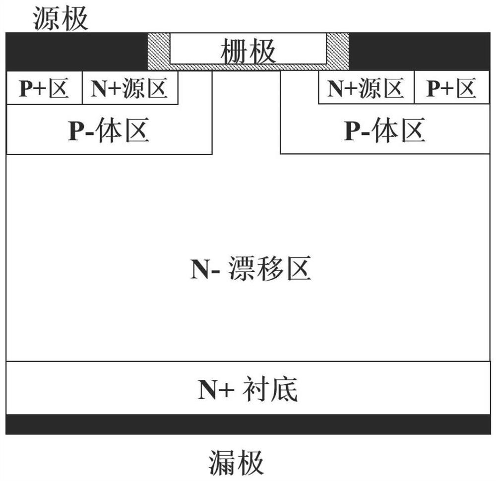
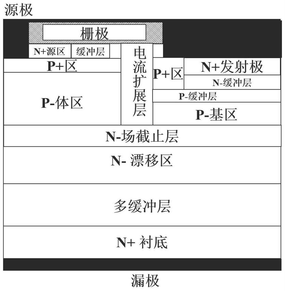
[0031] Such as figure 1 , 2 As shown, the present invention provides a power device anti-single event burning reinforcement structure, which is suitable for planar gate power VDMOSFET devices, figure 2 and figure 1 the difference lies in figure 2 The structure introduces an N-type multi-buffer layer, an N-type field stop layer and an integrated transistor structure under the neck electrode. Specifically, an N-type multi-buffer layer structure is set in the drain (cathode) electrode region of the semiconductor power device; a 0.5 μm groove is formed at the source (positive) electrode and the neck region electrode and a metal electrode is formed; the neck region An integrated transistor is arranged below the P-type body region and an N-type field stop layer is arrang...


PUM

PropertyMeasurementUnit
thicknessaaaaaaaaaa
depthaaaaaaaaaa
widthaaaaaaaaaa

Abstract

The invention discloses a power device single particle burnout resistant reinforced structure and a preparation method thereof. The method comprises the steps of arranging an N-type multi-buffer layer region structure in a drain electrode region of a semiconductor power device; forming a groove at a source electrode and a neck region electrode and forming a metal electrode; arranging an integrated transistor below the neck region; and arranging an N-type field stop layer between a P-type body region and a drift region. By adopting the technical scheme of the invention, the electric field peak value and collision ionization at the homojunction of a drift region and a substrate of the semiconductor power device can be greatly reduced, the number of carriers generated by avalanche multiplication caused by collision ionization is reduced, and meanwhile, the current density in the device is greatly reduced, so that the heat generated by a current heat effect is reduced, and the SEB safe working voltage of the device is remarkably improved.

Description

technical field [0001] The invention belongs to the technical field of power semiconductor devices, and in particular relates to a power device anti-single particle burning reinforcement structure and a preparation method based on an electric field modulation effect and an additional electrode structure. Background technique [0002] The power semiconductor device MOSFET has the advantages of fast switching speed, large output power, and simple driving circuit. It can realize power control and conversion in different ranges. It is widely used in power management of power electronic systems and has great development potential in the field of space applications. Silicon carbide power semiconductor device MOSFET usually has the characteristics of small size and high working voltage, and is susceptible to the influence of natural radiation environment in space, which causes single event effect (Single Event Effect, SEE), among which single event burnout (single event burnout, SEB...

Claims


Application Information

Patent Timeline
Patent Type & Authority Applications(China)
IPC IPC(8): H01L29/78H01L29/417H01L29/08H01L21/336
CPCH01L29/66712H01L29/7802H01L29/0865H01L29/41741Y02B70/10
Inventor 王颖毕建雄曹菲包梦恬于成浩李兴冀杨剑群
Owner HANGZHOU DIANZI UNIV
Why Eureka
Try Eureka