A kind of power device anti-single particle burnout reinforcement structure and preparation method

A power device, anti-single particle technology, applied in semiconductor/solid-state device manufacturing, semiconductor devices, electrical components, etc., can solve the problem of less research on anti-single particle reinforcement, increased device reverse leakage current density, carrier concentration Reduce and other problems to achieve the effect of improving anti-SEB performance, improving anti-SEB performance and reducing transient current

Active Publication Date: 2022-06-03
HANGZHOU DIANZI UNIV +1
View PDF0 Cites 0 Cited by
  • Summary
  • Abstract
  • Description
  • Claims
  • Application Information

AI Technical Summary

Problems solved by technology

For example, P + The method of expanding the source region can easily lead to a decrease in the carrier concentration in the channel region, which can reduce the forward conduction current density of the device; the introduction of the buffer layer reduces the peak electric field of the substrate junction and is accompanied by a decrease in the forward conduction resistance. increase; the introduction of the minority carrier lifetime recombination center will definitely cause an increase in the reverse leakage current density of the device, which will lead to an increase in power consumption, which does not meet the requirements of low power consumption for semiconductor devices in space applications, and the current resistance to power semiconductor devices The single particle burn-out reinforcement structure is mainly used in the case of low incident energy, and there are few studies on the anti-single particle reinforcement of high incident energy

Method used


Image

  • A kind of power device anti-single particle burnout reinforcement structure and preparation method
  • A kind of power device anti-single particle burnout reinforcement structure and preparation method
  • A kind of power device anti-single particle burnout reinforcement structure and preparation method

Examples


Embodiment Construction

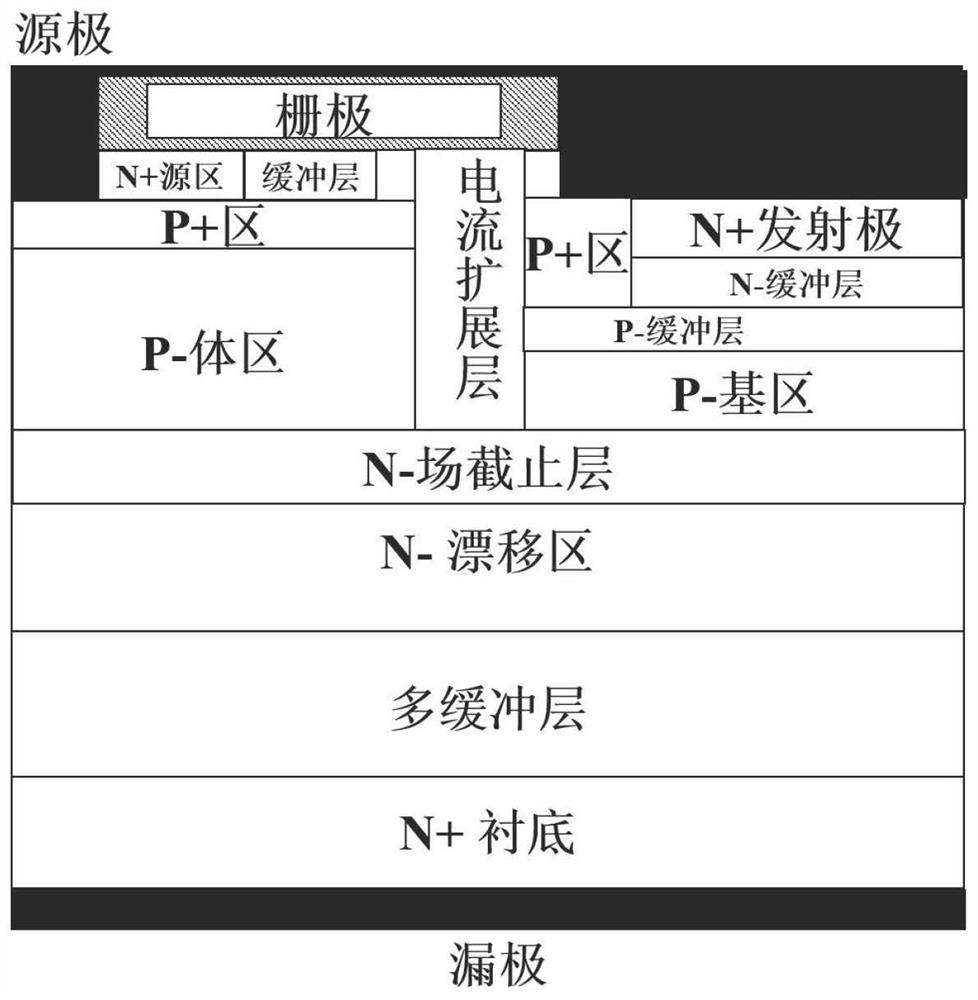
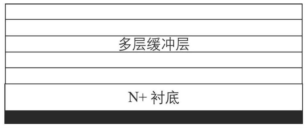
[0032] Further, the N-type multi-buffer layer structure has an epitaxial width of 11um and an overall epitaxial thickness of 15μm, which includes 5 layers of 3μm.

[0033] Further, the junction depth of the P-type body region is 5.2 μm and the width is 2.5 μm.

[0034] Further, the N-type field stop layer has an epitaxial width of 11 um and an overall epitaxial thickness of 0.4 μm, which includes two layers of 0.2 μm.

[0035] Further, the junction depth of the integrated transistor under the neck region electrode is 5.2 μm, the width is 1.5 μm, and the doping concentration is 2.4 μm

[0040] step 3, forming a drift region by epitaxy above the multi-buffer layer structure, as shown in FIG. 4;

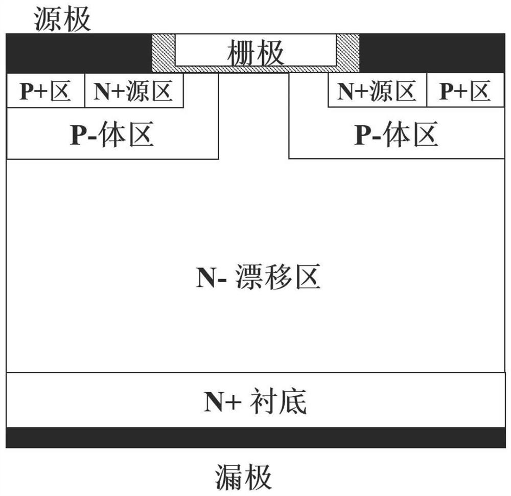
[0046] Select the 2000V plane gate power VDMOSFET device. The traditional structural cell has a width of 11 μm and a thickness of 16.5 μ


PUM

PropertyMeasurementUnit
thicknessaaaaaaaaaa
depthaaaaaaaaaa
widthaaaaaaaaaa

Abstract

The invention discloses a power device anti-single event burning reinforced structure electrode and a preparation method thereof. An N-type multi-buffer layer structure is arranged in the drain electrode region of a semiconductor power device; a groove is formed at the source electrode and the neck region electrode and A metal electrode is formed; an integrated transistor is arranged under the neck region; an N-type field stop layer is arranged between the P-type body region and the drift region. Adopting the technical scheme of the present invention can greatly reduce the electric field peak value and impact ionization at the drift region of the semiconductor power device and the substrate homojunction, and reduce the number of carriers generated by the avalanche multiplication caused by the impact ionization; The current density is greatly reduced, thereby reducing the heat generated by the thermal effect of the current, and the SEB safe working voltage of the device is significantly improved.

Description

A kind of power device anti-single particle burnout reinforcement structure and preparation method technical field The invention belongs to the technical field of power semiconductor devices, in particular to a kind of based on electric field modulation effect and additional electric An anti-single particle burnout reinforcement structure for a power device with a polar structure and a preparation method thereof. Background technique [0002] The power semiconductor device MOSFET has the advantages of fast switching speed, large output power, and simple driving circuit, which can realize Power control and conversion in different ranges, widely used in power management of power electronic systems There is huge development potential. Silicon carbide power semiconductor device MOSFET usually has the characteristics of small size and high operating voltage. The single event effect (SEE) is easily affected by the natural radiation environment in space. Particle burnout (...

Claims


Application Information

Patent Timeline
Patent Type & Authority Patents(China)
IPC IPC(8): H01L29/78H01L29/417H01L29/08H01L21/336
CPCH01L29/66712H01L29/7802H01L29/0865H01L29/41741Y02B70/10
Inventor 王颖毕建雄曹菲包梦恬于成浩李兴冀杨剑群
Owner HANGZHOU DIANZI UNIV
Why Eureka
Try Eureka