Supercharge Your Innovation With Domain-Expert AI Agents!

Thin film formation method and thin film formation apparatus

a thin film and formation method technology, applied in the direction of instruments, optical elements, vacuum evaporation coating, etc., can solve the problem of undermining the entire film forming efficiency, and achieve the effect of improving the film forming efficiency

Active Publication Date: 2019-09-17
SHINCRON KK
View PDF15 Cites 0 Cited by
  • Summary
  • Abstract
  • Description
  • Claims
  • Application Information

AI Technical Summary

Benefits of technology

The present invention provides a thin film formation method and apparatus that improve film formation efficiency by calculating the actual rate of thin film formation for a plurality of batches and using it as an estimated rate for forming another thin film of the same composition. This trial film formation can be omitted before performing real film formation, resulting in a more efficient overall film formation process. In addition, when forming an optical multilayer film by depositing different materials alternately for a plurality of times, it is preferable to calculate the actual rate of thin film formation at the most-initial-possible stage and reflect it in subsequent thin film formation to further improve the film formation efficiency.

Problems solved by technology

Therefore, lots of time and work have been necessary before the real film formation and that have resulted in undermining the entire film forming efficiency.

Method used


Image

  • Thin film formation method and thin film formation apparatus
  • Thin film formation method and thin film formation apparatus
  • Thin film formation method and thin film formation apparatus

Examples


Embodiment Construction

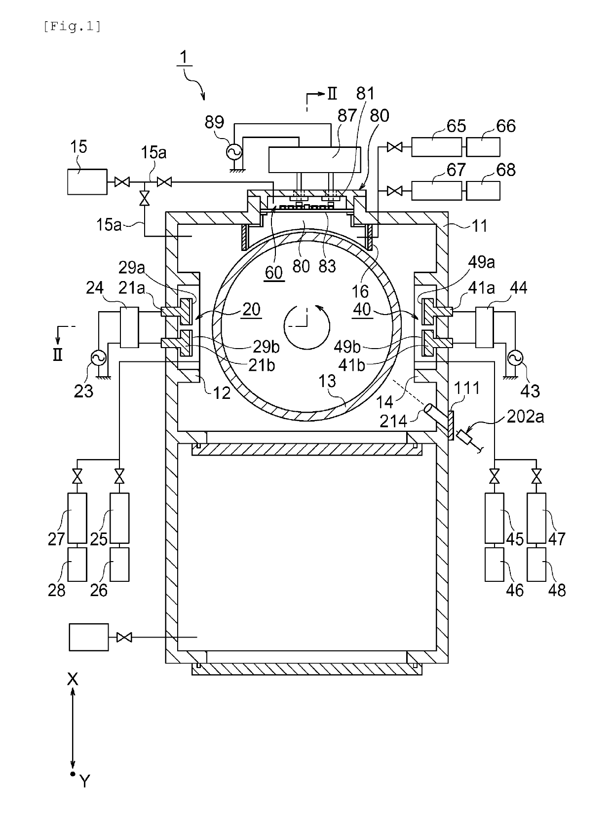
[0043]Blow, an embodiment of the invention explained above will be explained based on the drawings.

[0044]In the present embodiment, a sputtering apparatus 1 for performing magnetron sputtering as an example of sputtering is used but it is not limited to this, and sputtering apparatuses for performing double-pole sputtering and other well-known sputtering may be also used.

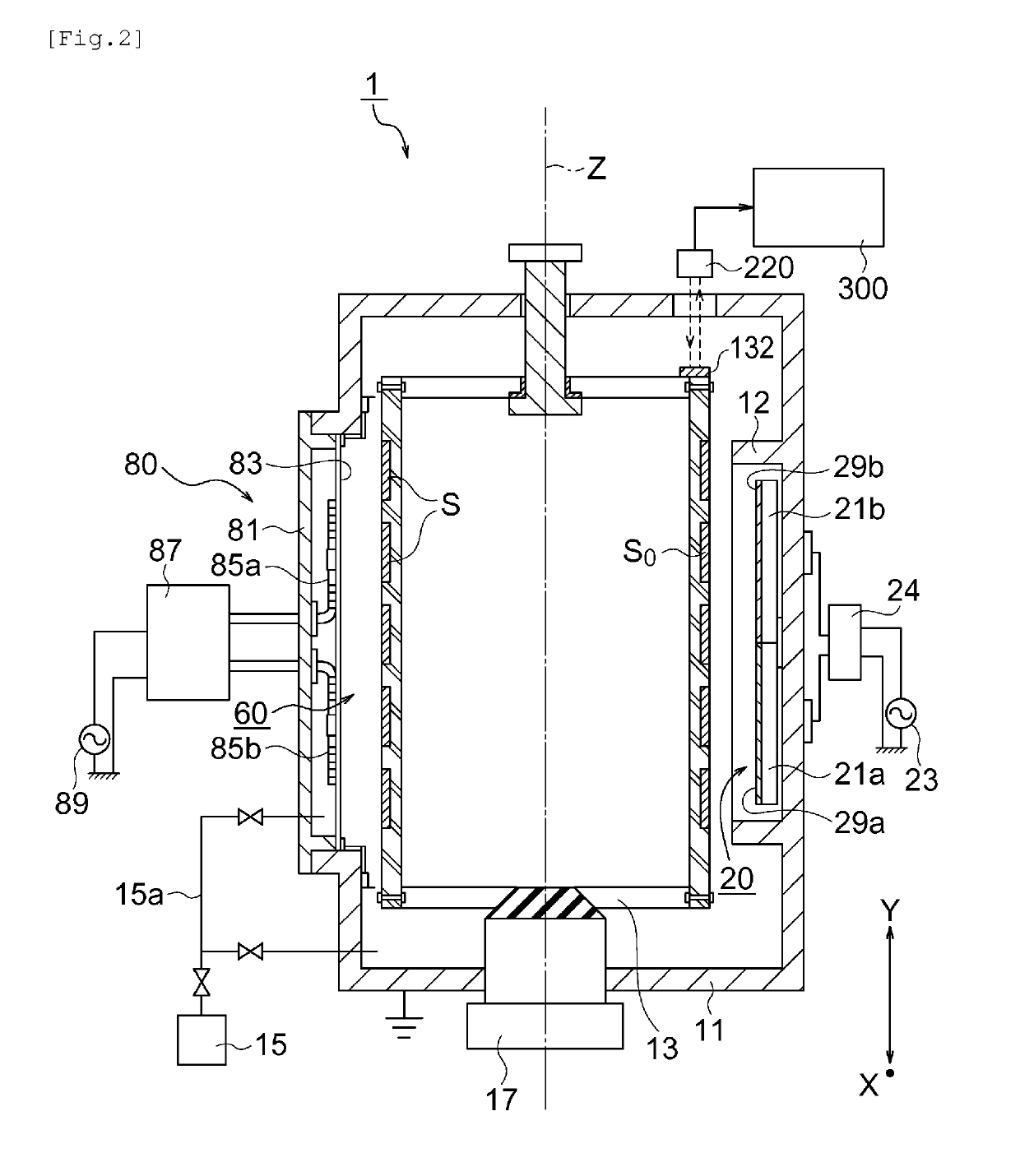
[0045]The sputtering apparatus 1 of the present embodiment is used for forming a multilayer film by depositing a plurality of single-layer thin films each having an intended film thickness on a substrate by repeating sputtering processing and plasma processing. In the present embodiment, sputtering processing and plasma processing are performed for one time when a rotation drum rotates once. Thereby, an ultrathin film having a film thickness of 0.01 nm to 1.5 nm or so in average is formed (thin film formation processing). By repeating the thin film formation processing for every rotation of the rotation drum, next u...


PUM

PropertyMeasurementUnit
thicknessaaaaaaaaaa
frequencyaaaaaaaaaa
pressureaaaaaaaaaa

Abstract

A thin film formation method is provided, by which needless film formation due to trial film formation is omitted and film formation efficiency can be improved. This invention is a method for sputtering targets to form a film A having an intended film thickness of T1 as the first thin film on a substrate and monitor substrate held and rotated by a rotation drum and, subsequently, furthermore sputtering the targets used in forming the film A to form a film C having an intended film thickness of T3 as the second thin film, which is another thin film having the same composition as the film A; comprising film thickness monitoring steps S4 and S5, a stopping step S7, an actual time acquisition step S8, an actual rate calculating step S9 and a necessary time calculating step S24.

Description

[0001]This application is a U.S. national phase filing under 35 U.S.C. § 371 of PCT Application. No. PCT / JP2011 / 063467, filed on Jun. 13, 2011 and therefore also claims priority under 35 U.S.C. § 119 to Japanese patent application no. 2010-228845 filed on Oct. 8, 2010.TECHNICAL FIELD[0002]The present invention relates to a thin film formation method and a thin film formation apparatus.BACKGROUND ART[0003]It has been conventionally carried out to form an optical thin film on a substrate surface by using a thin film formation apparatus for adhering a film material to the substrate surface by sputtering in order to manufacture interference filters, such as anti-reflection filters, half mirrors, a variety of bandpass filters and dichroic filters, and other optical products (patent document 1).RELATED ART DOCUMENTSPatent DocumentPatent Document 1: Japanese Patent Unexamined Publication (Kokai) No. 2001-133228SUMMARY OF THE DISCLOSED SUBJECT MATTER[0004]In methods of the related art for m...

Claims


Application Information

Patent Timeline
Patent Type & Authority Patents(United States)
IPC IPC(8): C23C14/54C23C14/50C23C14/34G02B5/28G02B1/11G02B1/115
CPCC23C14/547C23C14/3464C23C14/54C23C14/3492G02B5/28C23C14/545C23C14/505C23C14/34G02B1/11
Inventor HINATA, YOHEISAI, KYOKUYOOTAKI, YOSHIYUKISHIONO, ICHIROJIANG, YOUSONG
Owner SHINCRON KK
Features
  • R&D
  • Intellectual Property
  • Life Sciences
  • Materials
  • Tech Scout
  • Unparalleled Data Quality
  • Higher Quality Content
  • 60% Fewer Hallucinations
Learn More