Semiconductor light-emitting device and method for producing the same

a technology of light-emitting devices and semiconductors, which is applied in the direction of semiconductor devices, basic electric elements, electrical equipment, etc., can solve the problems of large change and difficult control of light intensity, and achieve the effect of easy adjustment of light intensity of output ligh

Active Publication Date: 2019-09-17
STANLEY ELECTRIC CO LTD
View PDF4 Cites 2 Cited by
  • Summary
  • Abstract
  • Description
  • Claims
  • Application Information

AI Technical Summary

Benefits of technology

[0005]The present invention has been made in view of the aforementioned problem, and an object of the present invention is to provide a semiconductor light-emitting device capable of easily adjusted the light intensity of output light and a method for producing a semiconductor light-emitting device having such a property as mentioned above.

Problems solved by technology

When light intensity is controlled by adjusting an amount of the black pigment mixed into the covering member together with the phosphor particles as in the light-emitting device described in Patent Literature 1, the control of the light intensity is difficult to achieve because a change in a mix rate of the pigment leads to a large change in light intensity.

Method used


Image

  • Semiconductor light-emitting device and method for producing the same
  • Semiconductor light-emitting device and method for producing the same
  • Semiconductor light-emitting device and method for producing the same

Examples


first embodiment

[0014]A preferred embodiment of the present invention will now be described below in detail. Note that substantially the same or equivalent parts are denoted by the same reference numerals in the following description and the accompanying drawings.

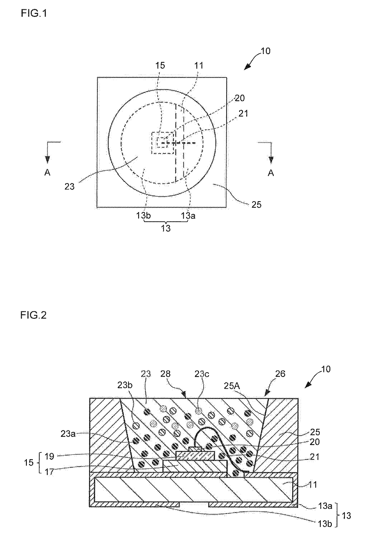
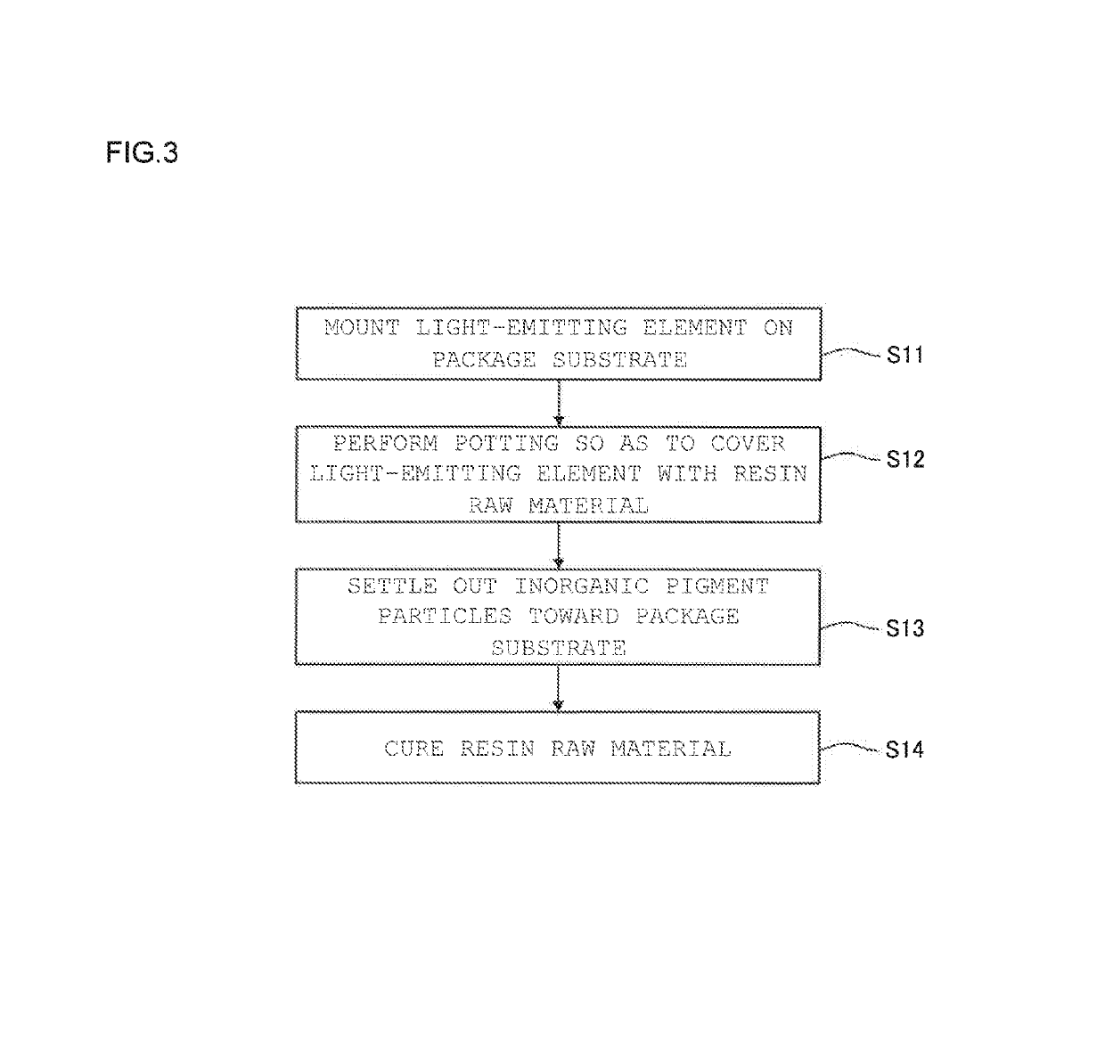
[0015]FIG. 1 shows an upper surface of a semiconductor light-emitting device 10 according to the first embodiment. As shown in FIGS. 1 and 2, an example of a package substrate 11 (mounting board), which serves as a substrate, is a glass epoxy substrate. A glass silicone substrate or a substrate made of a ceramic material such as alumina or AlN may also be employed as the package substrate 11. A connection electrode 13, which is formed, for example, by plating a conductor such as Cu on a surface of the package substrate 11, is provided on the surface of the package substrate 11.

[0016]The connection electrode 13 includes a p-connection electrode layer 13a and an n-connection electrode layer 13b. The connection electrode layers 13a and 13b ar...

second embodiment

[0077]FIG. 6 is a cross-sectional view of a semiconductor light-emitting device according to the second embodiment. The same elements as those in the semiconductor light-emitting device of the first embodiment will be denoted by the same reference numerals and the description thereof will be omitted.

[0078]A resin layer 23 includes a first resin layer 23d provided in contact with a light-emitting element 15, and a second resin layer 23e provided so as to cover the first resin layer 23d.

[0079]The first resin layer 23d is provided so as to cover or seal the light-emitting element 15. Specifically, the first resin layer 23d is provided so as to cover an upper surface and side surfaces of the light-emitting element 15. A conductive wire 21 is also sealed by the first resin layer 23d. The first resin layer 23d is a layer containing a resin as a main component, such as a silicone resin, and inorganic pigment particles 23a.

[0080]The second resin layer 23e is formed so as to cover an upper...


PUM

PropertyMeasurementUnit
particle sizeaaaaaaaaaa
wavelengthaaaaaaaaaa
particle sizeaaaaaaaaaa

Abstract

Provided are a semiconductor light-emitting device capable of easily adjusting the light intensity of output light and a method for producing such a semiconductor light-emitting device. The semiconductor light-emitting device includes: a substrate; a light-emitting element mounted on the substrate; and a seal layer provided on the substrate so as to cover the light-emitting element. The seal layer contains resin and inorganic pigment particles. The inorganic particles have an average particle size of 1 □m or larger and 50 □m or smaller in a volumetric basis particle size distribution by a laser diffraction scattering particle size distribution measurement method. The inorganic particles distributed at a concentration becoming thicker in a direction toward said substrate.

Description

BACKGROUND OF THE INVENTION1. Field of the Invention[0001]The present invention, in particular, relates to a semiconductor light-emitting device including a semiconductor element such as a light-emitting diode (LED) and a method for producing such a semiconductor light-emitting device.2. Description of the Related Art[0002]Light intensities of light-emitting elements have been improved in its output intensities in recent years. However, light-emitting elements having low light intensities, are also required for use in indicators, for example. In view of this, light-emitting devices having low light intensities have been provided by adjusting light intensities of high light intensity light-emitting elements.[0003]Patent Literature 1, for example, discloses a white light-emitting device in which variations in luminance are adjusted by mixing a black pigment, as a light attenuation material, into a covering or seal member containing phosphor particles mixed therein (Japanese Patent App...

Claims


Application Information

Patent Timeline
Patent Type & Authority Patents(United States)
IPC IPC(8): H01L33/56H01L33/00H01L33/36H01L33/50
CPCH01L33/36H01L33/56H01L33/005H01L33/501H01L33/48H01L33/52H01L33/62
Inventor OKUBO, TSUTOMU
Owner STANLEY ELECTRIC CO LTD
Why Eureka
Try Eureka