
Method of manufacturing large area graphene and graphene-based photonics devices

a graphene-based photonics and graphene-based technology, applied in the direction of instruments, fibre light guides, cladded optical fibres, etc., can solve the problems of poor quantum efficiency, difficult fabrication, limited bandwidth, etc., and achieves reduced saturation intensity, wide bandwidth, and easy production

Inactive Publication Date: 2019-10-22
NASA
View PDF4 Cites 3 Cited by
  • Summary
  • Abstract
  • Description
  • Claims
  • Application Information

AI Technical Summary

Benefits of technology

[0010]In one embodiment, a novel method of fabrication of large area monolayer and multi-layer graphene samples of optical quality for a mode locking process, are achieved. The graphene-based saturable absorber of the present invention is easy to produce, has the advantages of a much wider bandwidth, lower saturation intensity, tunable modulation depth, ultrafast recovery time, and much higher optical damage threshold, thus, producing higher energies (10's nJ) and femtosecond pulses with a repetition rate on order of 100's MHz.
[0011]In one embodiment, the present invention takes advantage of the unique optical and electrical properties of graphene, as well as enhances the responsivity with plasmonic effects of graphene-grating metamaterials, to enable spectral imaging in the THz range important for applications in astrophysics, gas analysis for planetary bodies, thermal imaging for homeland security, and remote sensing.

Problems solved by technology

Silicon (Si) photodetectors do not meet these requirements since they have poor quantum efficiency for wavelengths greater than 1.1 μm and have low bandwidth, such as <500 MHz.
This type of passive mode locker produces exceptional results but is difficult to fabricate, expensive and limited to bandwidth.
Further, other potential remote sensing instruments with requirements to perform spectroscopic measurements, such as those using methane, need specific wavelengths most likely in the mid-infrared (IR) to long-wave IR (LWIR) bands, to match the absorption spectra of the species being studied, which are difficult to provide.
Current spectroscopic techniques which offer broadband, high-resolution capability, require cumbersome optics with moving parts and / or sophisticated cryogenic cooling to obtain the necessary resolving power and sensitivity, and thus, are not suitable for air or space vehicle applications whose platforms require strict size and weight requirements.
Further, commercial charge-coupled device (CCD) spectrometers are not available in the terahertz spectral range, and which can operate at room temperature.

Method used


Image

  • Method of manufacturing large area graphene and graphene-based photonics devices
  • Method of manufacturing large area graphene and graphene-based photonics devices
  • Method of manufacturing large area graphene and graphene-based photonics devices

Examples


Embodiment Construction

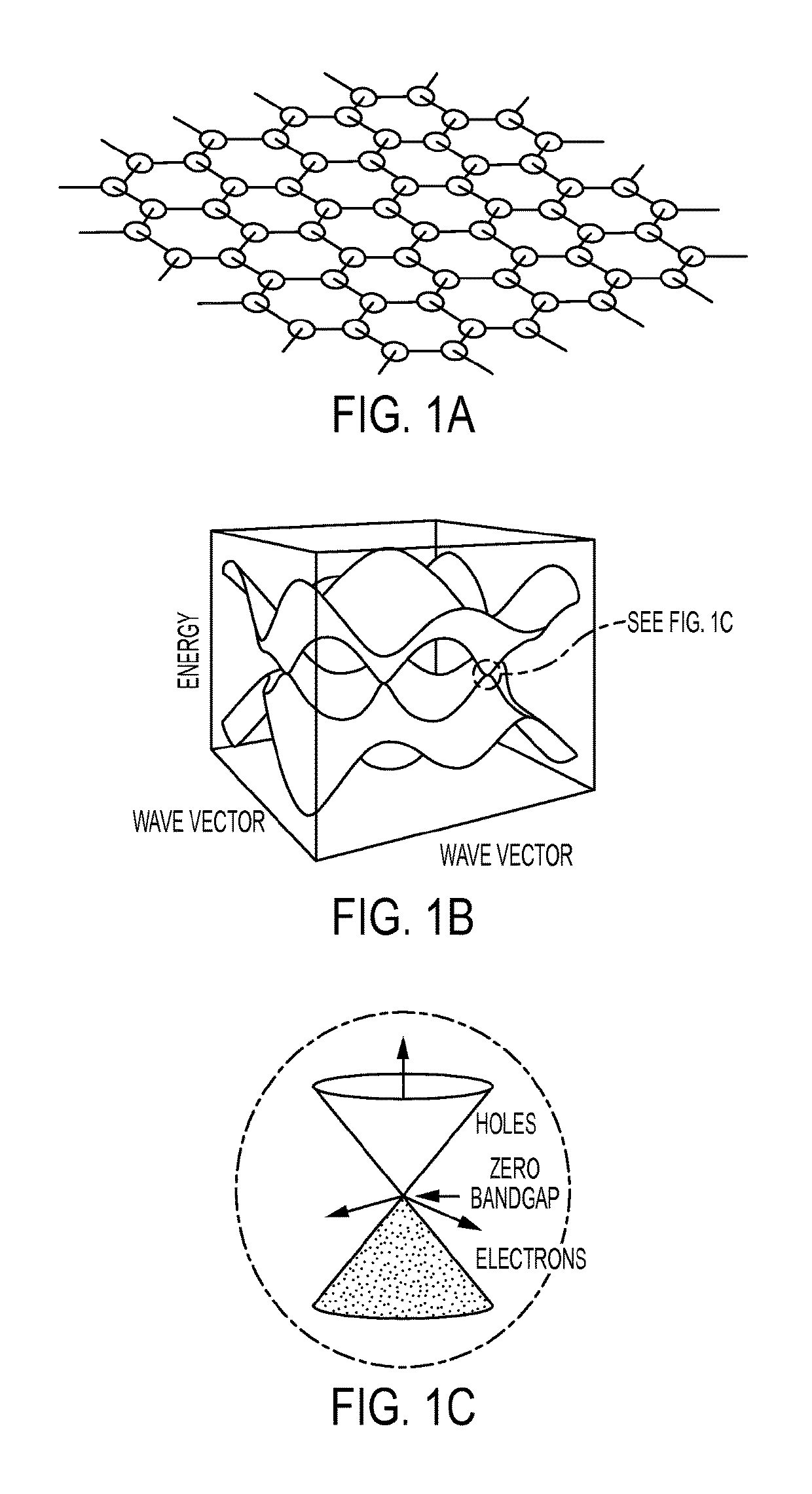
[0054]The present invention relates to a method of manufacturing large area graphene, for use in graphene-based photonics devices, and which are used in a variety of applications. The present invention includes the fabrication of large area monolayer and multi-layer graphene samples of optical quality for a mode locking process. The present invention includes production of an ultrafast laser ranging instrument and an ultrawide bandwidth detector based on graphene as a saturable absorber, to demonstrate mode locking locked laser pulses in a laser application.

[0055]In addition, the present invention takes advantage of the unique optical and electrical properties of graphene, as well as enhances the responsivity with plasmonic effects of graphene-grating metamaterials, to enable spectral imaging in the THz range important for applications in astrophysics, gas analysis for planetary bodies, thermal imaging for homeland security, and remote sensing.

[0056]Graphene is a flat single layer c...


PUM

PropertyMeasurementUnit
photo responsivityaaaaaaaaaa
NIR) wavelengthaaaaaaaaaa
wavelengthsaaaaaaaaaa

Abstract

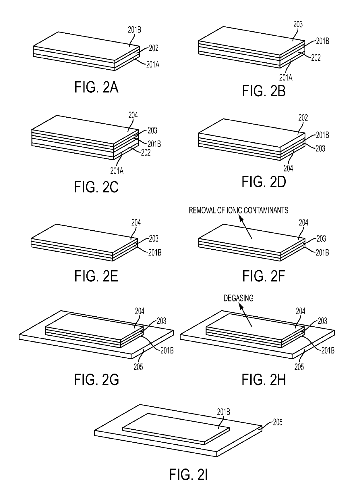
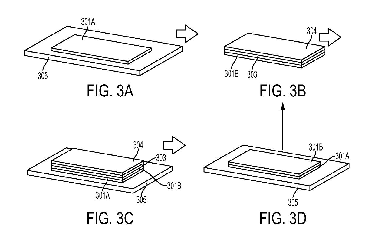
The present invention relates to a method of manufacturing large area graphene for graphene-based photonics devices such as bolometric graphene detectors, or for use as a saturable absorber in ultra-high bandwidth detectors for producing ultrafast laser pulses. The method includes: growing a first graphene layer on one side of a metal substrate, and a second graphene layer on another side of the metal substrate; coating the first graphene layer with a plurality of resist layers including a low molecular weight polymethylmethacrylate, and a high molecular weight polymethylmethacrylate; removing the second graphene layer and the metal substrate to reveal the first graphene layer; disposing the first graphene layer on an optical substrate; and removing the plurality of resist layers from the first graphene layer to reveal a final graphene layer, which can be used as the basis to manufacture a multilayer graphene structure for graphene detectors.

Description

BACKGROUND OF THE INVENTION[0001]1. Field of the Invention[0002]The present invention relates to a method of manufacturing large area graphene, and the resulting graphene-based photonics devices, which are used in a variety of applications.[0003]2. Description of the Related Art[0004]A Laser Imaging and Detection and Ranging (LIDAR) system is a remote sensing technology that provides for the detection, identification, and the precision measurement of the range of a target in military missions, using a laser to illuminate the target and analyze the reflected light. The components of a scanning LIDAR system include a laser, a scanner and optics (i.e., oscillating plane minors, a combination with a polygon mirror, a dual axis scanner etc.), photodetectors and receiver electronics, and position and navigation systems (i.e., Global Positioning System (GPS) and Inertial Measurement Unit (IMU)). Typically, a laser with shorter pulses achieves better target resolution, provided the LIDAR re...

Claims


Application Information

Patent Timeline
Patent Type & Authority Patents(United States)
IPC IPC(8): B32B9/00F21V8/00G02B6/36G02F1/35C01B32/186C01B32/194G02B6/02C23C16/26C23C16/01G02F1/01B82Y20/00B82Y40/00
CPCC01B32/186C01B32/194G02B6/3624G02F1/3523C23C16/01G02F1/011C23C16/26G02B6/02G02B6/0008B82Y40/00B82Y20/00
Inventor SULTANA, MAHMOODALI, MARY J.YU, ANTHONY W.
Owner NASA
Learn More