

Method for manufacturing a multilayer structure for hosting electronics
a multi-layer structure and electronics technology, applied in the field of electronics, can solve the problems of not always being completely isolated, not always functioning completely, and not always being able to achieve the desired effect, and the layout of the connection itself may be rather complex, and the physical connection established and the connection layout may be difficult to achiev
- Summary
- Abstract
- Description
- Claims
- Application Information
AI Technical Summary
Benefits of technology
Problems solved by technology
Method used
Image

Examples
Embodiment Construction
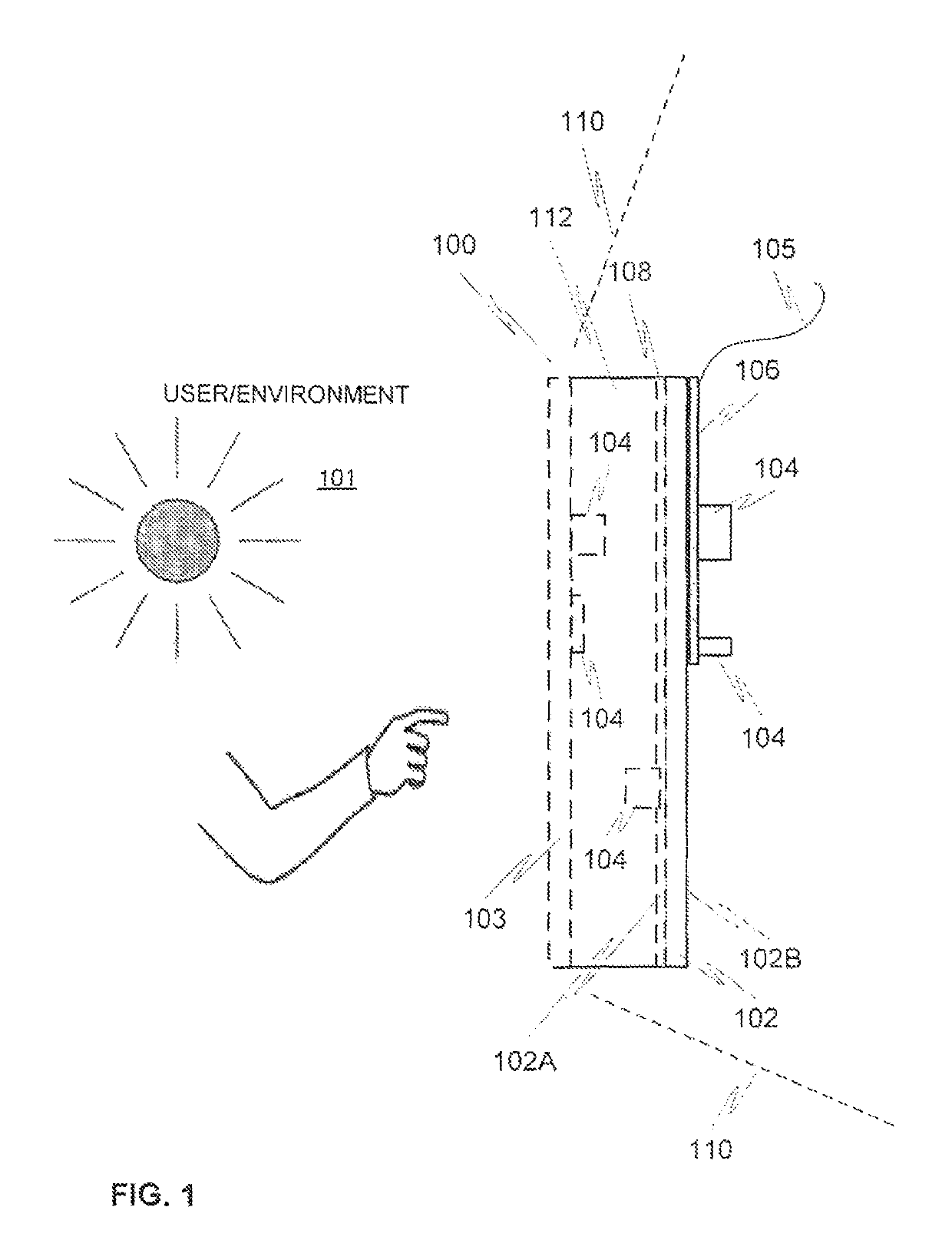
[0093]FIG. 1 illustrates, by means of a cross-sectional side view, many general concepts of various embodiments of the present invention via one, merely exemplary, realization of a multilayer structure at 100. Item 101 refers to potential use environment (outdoors, indoors, in-vehicle, etc.) and human user (if any) of the structure 100 located in the environment, whereas item 110 indicated by broken contour lines refers to a host device or host structure 110.
[0094]The finished multilayer structure 100 may indeed establish an end product of its own, e.g. electronic device, or be disposed in a host device as an aggregate part or module. It 100 may naturally comprise a number of further elements or layers not shown in the figure.
[0095]The structure 100 contains at least one substrate film 102 accommodating a number of electronic components 104 on a second side 102B thereof (which may in many, but not all, feasible use cases thus be considered as back exterior side, when the first side,...
PUM
| Property | Measurement | Unit |
|---|---|---|
| transmittance | aaaaa | aaaaa |
| transmittance | aaaaa | aaaaa |
| transmittance | aaaaa | aaaaa |
Abstract
Description
Claims
Application Information