
Active-matrix display device and method for driving the same

a display device and active matrix technology, applied in the direction of instruments, static indicating devices, etc., can solve the problems of complex and larger-scale configuration of components such as the scanning signal line driver circuit, display portion suffers from display irregularities, and cannot provide satisfactory display

Active Publication Date: 2019-11-19
SHARP KK
View PDF8 Cites 0 Cited by
  • Summary
  • Abstract
  • Description
  • Claims
  • Application Information

AI Technical Summary

Benefits of technology

The invention provides an active-matrix display device that can display images without any irregularities, even if there are scanning signal lines with non-uniform lengths. This is achieved by using multiple analog switches to sample the scanning clock signal and applying it to the scanning signal lines. This leads to a more uniform voltage reduction in the display pixels, inhibiting any luminance difference from occurring. This method helps to avoid the need for additional circuits and complexity.

Problems solved by technology

As a result, the display portion suffers from display irregularities, such as differences in luminance, and cannot provide satisfactory display.
However, an attempt to generate such a scanning signal on the basis of a configuration disclosed in International Publication WO 2016 / 163299 (see FIGS. 3 and 18 of the publication) requires a plurality of additional control signals, resulting in more complex and larger-scale configurations of components such as the scanning signal line driver circuit (i.e., the gate driver).

Method used


Image

  • Active-matrix display device and method for driving the same
  • Active-matrix display device and method for driving the same
  • Active-matrix display device and method for driving the same

Examples


first embodiment

1. First Embodiment

1.1 Overall Configuration

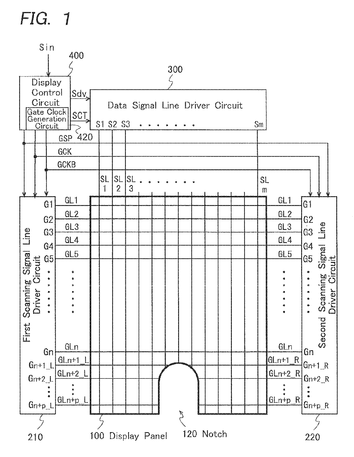
[0028]FIG. 1 is a block diagram illustrating an overall configuration of a liquid crystal display device according to a first embodiment. This liquid crystal display device includes a display panel 100, which is an active-matrix display portion, first and second scanning signal line driver circuits (also referred to as “gate drivers”) 210 and 220, a data signal line driver circuit (also referred to as a “source driver”) 300, and a display control circuit 400. The display control circuit 400 is externally provided with an input signal Sin, which includes an image signal representing an image to be displayed and a timing control signal for displaying the image.

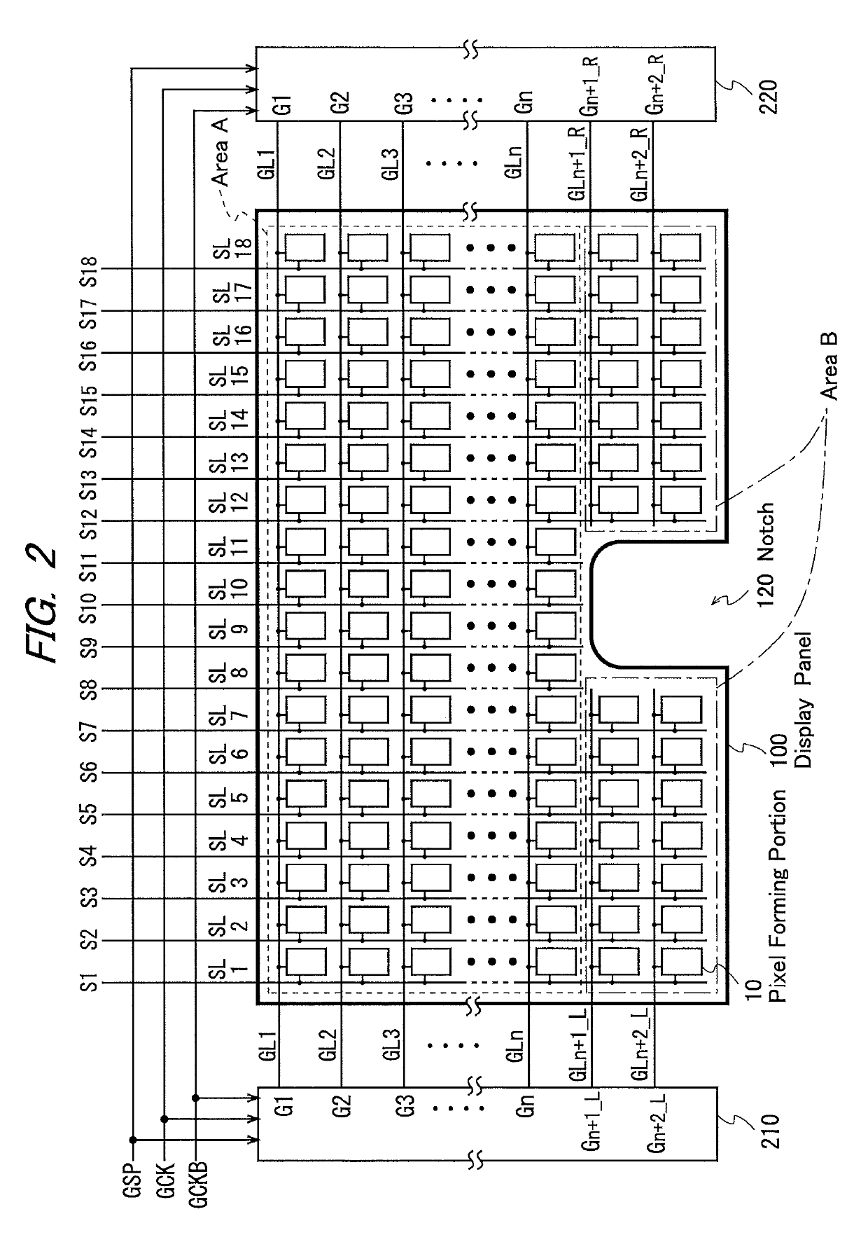
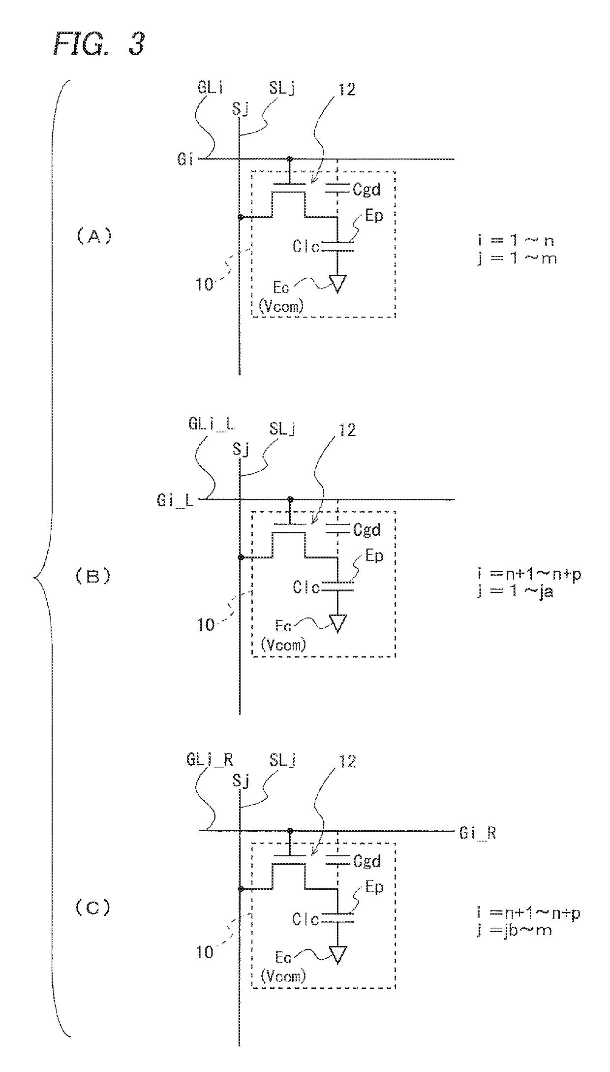
[0029]FIG. 2 is a diagram describing a configuration of the display panel 100 in the first embodiment. The display panel 100 has provided therein a plurality (m) of data signal lines (also referred to as “source lines”) SL1 to SLm, a plurality (n+p) of scanning signal lines (also refer...

second embodiment

2. Second Embodiment

[0058]Next, an example of the liquid crystal display device in which the circuit that corresponds to the waveform control circuit 423 in the first embodiment is provided between the display control circuit and the scanning signal line driver circuit will be described as a second embodiment. The present embodiment differs from the first embodiment in the configuration that rounds the original clock pulses in order to equalize the pixel voltage reduction amount ΔVp, but since other configurations are the same as in the first embodiment, the same or corresponding components are denoted by the same reference characters, and any detailed descriptions thereof will be omitted.

[0059]FIG. 11 is a diagram describing the configuration of the liquid crystal display device according to the present embodiment. In the present embodiment, as in the first embodiment, the display panel 100 is an active-matrix display panel and has the notch 120, as shown in FIG. 11. However, in th...

third embodiment

3. Third Embodiment

[0065]While in the first and second embodiments, the display panel 100 is configured to have the notch 120 as shown in FIGS. 1 and 2, other active-matrix liquid crystal display devices with non-rectangular display panels can also have a feature that controls the waveforms of the gate clock signals GCK and GCKB in order to equalize the pixel voltage reduction amount ΔVp. Accordingly, as a third embodiment, a liquid crystal display device with a circular display panel will be described below. In the following, elements of the present embodiment that are the same as or correspond to those of the first embodiment are denoted by the same reference characters, and any detailed descriptions thereof will be omitted.

[0066]FIG. 14 is a diagram describing the configuration of the liquid crystal display device according to the third embodiment. In the present embodiment, unlike in the first and second embodiments, the display panel 100 of the liquid crystal display device has...


PUM


Abstract

This application discloses an active-matrix display device capable of providing satisfactory display free from display irregularities on a non-rectangular display portion, such as a notched display portion, while avoiding an increased circuit scale and other adverse factors. In such an active-matrix liquid crystal display device including a notched display portion, pulses of gate clock signals GCK and GCKB corresponding to pulses of scanning signals are subjected to waveform rounding in accordance with time constants of scanning signal lines to which the scanning signals are to be applied. As a result, the waveforms of all scanning signals to be applied to the scanning signal lines are rounded to almost the same degree. Thus, each pixel forming portion is approximately equal in pixel voltage reduction amount ΔVp upon turning off of a pixel switching element.

Description

BACKGROUND OF THE INVENTION1. Field of the Invention[0001]The present invention relates to active-matrix display devices, more specifically to an active-matrix display device including a plurality of pixel forming portions arranged in a matrix, each of which includes a switching element, such as a thin-film transistor, and data holding capacitance, such as pixel capacitance, and the invention also relates to a method for driving the same.2. Description of the Related Art[0002]In an active-matrix liquid crystal display device, a plurality of data signal lines (also referred to as “source lines”), a plurality of scanning signal lines (also referred to as “gate lines”) crossing the data signal lines, and a plurality of pixel forming portions arranged in a matrix along the data signal lines and the scanning signal lines are formed in a display portion such as a liquid crystal panel.[0003]In such an active-matrix liquid crystal display device, each pixel forming portion includes a transi...

Claims


Application Information

Patent Timeline
Patent Type & Authority Patents(United States)
IPC IPC(8): G09G3/36
CPCG09G3/3677G09G2310/06G09G2310/08G09G2310/0283G09G2320/0219G09G2310/0286G09G2300/0876G09G3/3648G09G2300/0426G09G2310/0281
Inventor SASAKI, OSAMU
Owner SHARP KK
Learn More