1T1D DRAM cell and access method and associated device for DRAM

a random access memory and access method technology, applied in the field of memory elements of random access memory, can solve problems such as poor performance of all, and achieve the effect of enhancing the performance of all

Active Publication Date: 2019-11-19
TANG CHAO JING
View PDF18 Cites 3 Cited by
  • Summary
  • Abstract
  • Description
  • Claims
  • Application Information

AI Technical Summary

Benefits of technology

[0011]The present invention manufactures DRAM with standard semiconductor process technology, and its structure is consisting of one transistor and one diode, wherein the depletion capacitance of diode is utilized to form a capacitor. Furthermore, it cooperates with access circuit corresponding to SRAM. The performance of all is thus enhanced.
[0012]The present invention reduces the number of used transistors for elevating the integrated intensity for SRAM and expects using only three transistors in standard CMOS process technology to implement SRAM to overcome the stability of storage status and reduce the power consumption of memory, further, to implement related circuits and the corresponding access circuit and system.
[0013]On a motherboard of Personal Computer (PC), access time is greatly increased when DRAM operates in the period of reading data, and might be increased in the period of refreshing memory. Therefore, the Central Processing Unit (CPU) cannot immediately retrieve data from DRAM, thus all operating commands of CPU will be enforced stop after a data reading command. There are solutions for abovementioned problem is to switch threads, or add more space of cache memory in CPU, or use a cache memory with more hierarchies. One of the problems will be solved by the present invention is making SRAM be able to replace DRAM, or greatly enhance the performance of DRAM and reduce the hierarchy of cache memory.
[0014]For the motherboard of PC, the CPU has cache memory whose hardware circuit is implemented by SRAM. Another problem will be solved by the present invention is using this technology to implement cache memory for reducing layout area and power consumption.

Problems solved by technology

Furthermore, the corresponding access circuit is relatively complicate which results in a poor performance of all.

Method used


Image

  • 1T1D DRAM cell and access method and associated device for DRAM
  • 1T1D DRAM cell and access method and associated device for DRAM
  • 1T1D DRAM cell and access method and associated device for DRAM

Examples


first embodiment

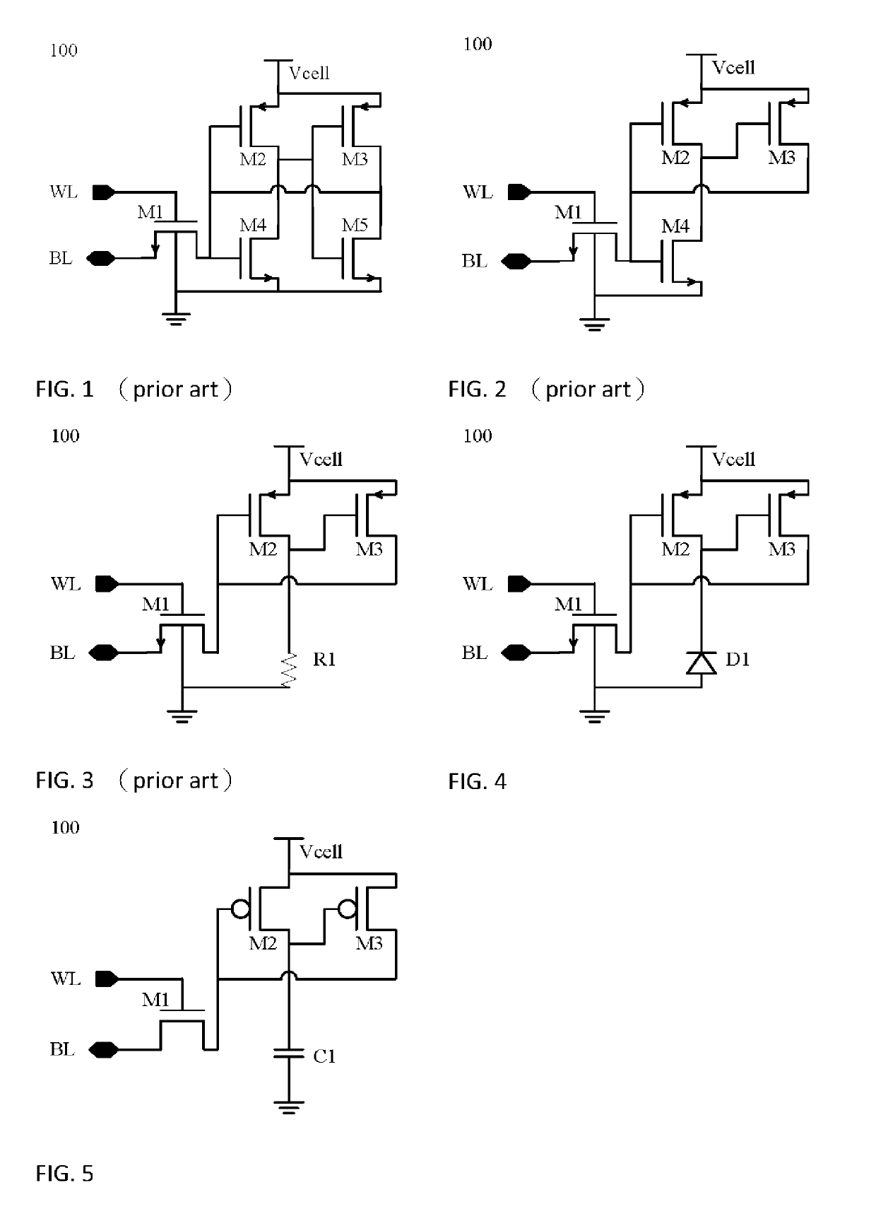
[0056]the present invention: Refer to FIG. 4, an SRAM cell 100 is consisting of three transistors and one diode under transistor-level design, which will be stated as “3T1D SRAM cell” in the following. In FIG. 4, M1 to M3 are a MOSFET respectively stated as first to third transistor, wherein M1 is an NMOS while M2 and M3 are a PMOS, and D1 is a diode comprising an anode and a cathode. The anode is called a first connective point and the cathode is called a second connective point. The other nodes are similar with those in FIG. 1-FIG. 3.

[0057]The 3T1D SRAM cell 100 comprises a data transmission node, a transmission control node, a cell power terminal point, a ground terminal point, a first transistor, a second transistor, a third transistor, and a first diode.

[0058]The wiring net of said first transistor is described as follows: the source terminal couples to said data transmission node; the gate terminal couples to said transmission control node; the drain terminal connects to gate ...

second embodiment

[0064]the present invention: refer to FIG. 5, an SRAM cell 100 is consisting of three transistors and one capacitor under transistor-level design, which will be stated as “3T1C SRAM cell” in the following. Please note that this embodiment will be easier to implemented by Silicon-On-Insulator (SOI) process technology, and the produced transistor has no bulk. In FIG. 5, M1 to M3 are a MOSFET respectively stated as first to third transistor, wherein M1 is an NMOS while M2 and M3 are a PMOS, and C1 is a capacitor comprising a first connective point and a second connective point. The other nodes are similar with those in FIG. 1-FIG. 4.

[0065]The 3T1C SRAM cell comprises a data transmission node, a transmission control node, a cell power terminal point, a ground terminal point, a first transistor, a second transistor, a third transistor, and a first capacitor. The wiring net can be referred to aforementioned 3T1D SRAM cell 100, the detailed description is omitted here.

[0066]The 3T1C SRAM c...

third embodiment

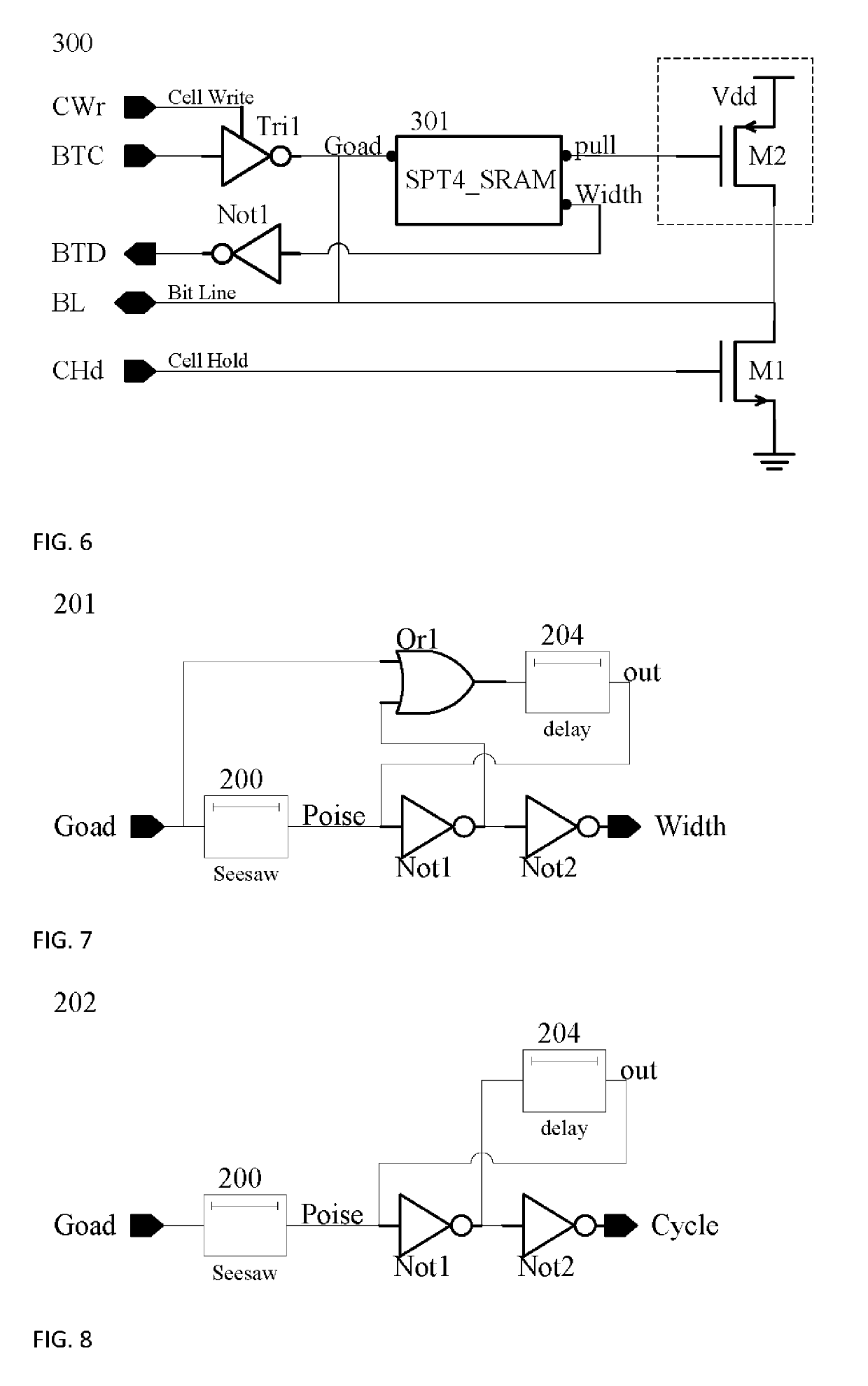
[0069]the present invention: refer to FIG. 6, which is an exemplary circuit diagram, wherein the Cell Access and Hold 300 (CAH 300) is a circuit diagram combining transistor-level design, gate-level design and function blocks. M1 and M2 are a MOSFET respectively stated as first and second transistor, wherein M1 is NMOS while M2 is PMOS. In FIG. 6, Tri1 is tri-state gate; Not1 is NOT gate.

[0070]SPT_SRAM 301 is a function block diagram, arranged to detect BL. When BL is slightly increased to high voltage from a relatively low voltage, a rail-to-rail high voltage is quickly outputted. This will be discussed in the following paragraphs. In FIG. 6, “Goad” is a first input connective point, “Width” is a first output connective point, and “pull” is a second output connective point.

[0071]An input node: Cell Write, hereinafter “CWr”, is a control node arranged to start function of cell write, and change storage status of aforementioned memory element.

[0072]An input node: Cell Hold, hereafter...


PUM


Abstract

The beginning of using Complementary Metal-Oxide-Semiconductor (CMOS) process technology to implement Static Random-Access Memory (SRAM) which transistor number is six. And then reducing transistor number for increasing integration density, but it will diminish the stability of memory, and also may enhance the complexity of access circuit, thus increasing the power consumption. For increasing the integration density of SRAM, and according to the electrical characteristics of reduced transistor number therefore designing the memory possess low power consumption and its corresponding circuits, and then implementing an access system. If electrical characteristic of the other various memories are similar to SRAM, such as Dynamic Random-Access Memory (DRAM), so they can also use the corresponding access circuit of SRAM.

Description

BACKGROUND OF THE INVENTION1. Field of the Invention[0001]The present invention relates to a memory element of random-access memory, and more particularly, to semiconductor process technologies for implementing static random-access memories and dynamic random-access memories, and further for implementing the corresponding access circuits and access systems.2. Description of the Prior Art[0002]The earliest CMOS process technology for implementing Static Random-Access Memory (SRAM) utilizes six transistors, five transistors, then four transistors in advancement. Currently, Dynamic Random-Access Memory (DRAM), or more specifically, its structure is consisting of one transistor and one capacitor to form a storage cell, wherein DRAM is manufactured by special semiconductor process technology. Furthermore, the corresponding access circuit is relatively complicate which results in a poor performance of all.[0003]The applicant has published the basic knowledge regarding the present inventio...

Claims


Application Information

Patent Timeline
Patent Type & Authority Patents(United States)
IPC IPC(8): G11C11/419G11C11/418G11C11/408G11C11/412G11C11/4094G11C11/4074G11C11/405G11C7/12G11C5/14G11C11/406G11C11/409
CPCG11C11/419G11C11/408G11C11/418G11C11/406G11C11/4074G11C11/4087G11C11/4094G11C11/409G11C11/405G11C11/4085G11C5/147G11C7/12G11C11/412G11C2211/4066G11C11/417G11C11/4096G11C11/4093G11C7/106G11C7/1069G11C7/1087G11C7/1096G11C7/1006G11C11/413G11C11/4076
Inventor TANG, CHAO-JING
Owner TANG CHAO JING
Why Eureka
Try Eureka