

Phase change memory and fabrication method thereof
a technology of phase change memory and fabrication method, which is applied in the direction of digital storage, semiconductor devices, instruments, etc., can solve the problems of slow read/write speed, low read/write efficiency, and drawbacks of phase change memory
- Summary
- Abstract
- Description
- Claims
- Application Information
AI Technical Summary
Benefits of technology
Problems solved by technology
Method used
Image

Examples
Embodiment Construction
[0013]Reference will now be made in detail to the exemplary embodiments of the disclosure, which are illustrated in the accompanying drawings. Wherever possible, the same reference numbers will be used throughout the drawings to refer to the same or similar parts.
[0014]The present disclosure provides a phase change memory and the fabrication method thereof to increase the read / write speed and improve the performance of the phase change memory.
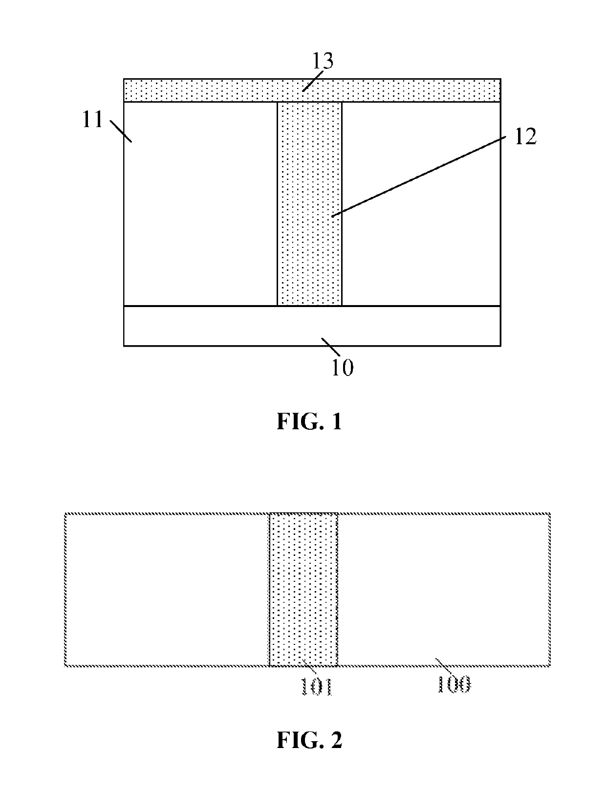
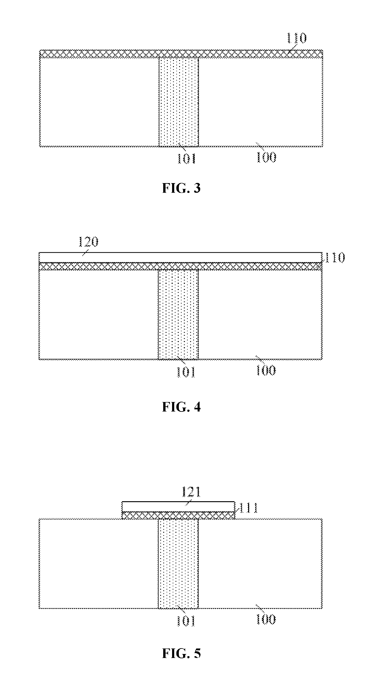
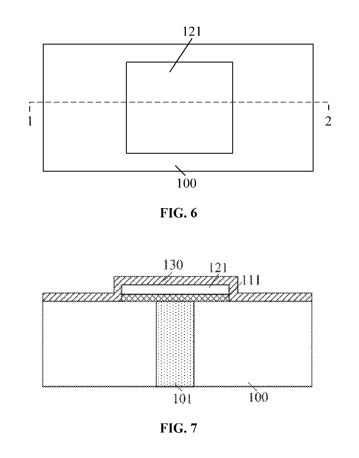
[0015]For example, a phase change memory may be fabricated by: forming a heating layer on a substrate; forming a phase change layer on one sidewall surface of the heating layer. in one embodiment, only one sidewall surface of the heating layer is in contact with the phase change layer. The thickness of the heating layer may be made smaller than the minimum size of the heating layer when forming the heating layer. As such, the contact area between the phase change layer and the heating layer can be made sufficiently small, and only a small porti...
PUM
| Property | Measurement | Unit |
|---|---|---|
| thickness | aaaaa | aaaaa |
| thickness | aaaaa | aaaaa |
| side length | aaaaa | aaaaa |
Abstract
Description
Claims
Application Information