

Laminated ceramic chip component including nano thin film layer, manufacturing method therefor, and atomic layer vapor deposition apparatus therefor
a technology of which is applied in the manufacture of capacitors, final products, fixed capacitors, etc., can solve the problems of difficult fixation, inconvenient atomic layer deposition apparatus for forming nano thin film layer, and inability to separate laminate ceramic capacitors from mounting nozzles
- Summary
- Abstract
- Description
- Claims
- Application Information
AI Technical Summary
Benefits of technology
Problems solved by technology
Method used
Image

Examples
Embodiment Construction
[0043]Hereinafter, a laminated ceramic chip component provided with a nano thin film layer, a method for manufacturing the same and an atomic layer deposition apparatus therefor according to the present disclosure are described in detail with reference to the accompanying drawings.
[0044]First of all, a laminated ceramic chip component provided with a nano thin film layer according to one embodiment of the present disclosure is described.
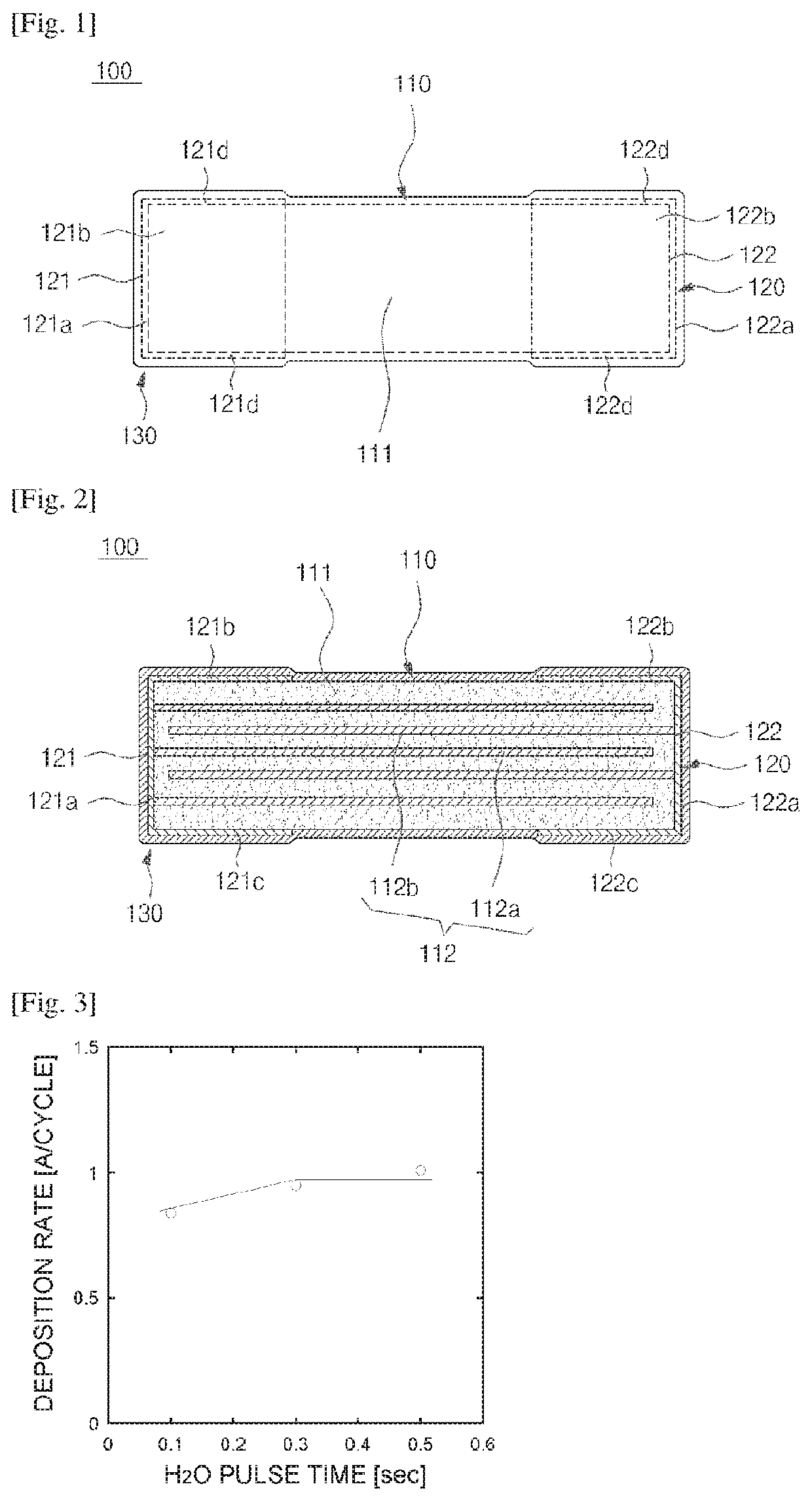
[0045]FIG. 1 is a plane view of a laminated ceramic capacitor provided with a nano thin film layer according to one embodiment of the present disclosure. FIG. 2 is a vertical sectional view taken along the line A-A in FIG. 1.
[0046]Referring to FIG. 1 and FIG. 2, a laminated ceramic chip component 100 according to one embodiment of the present disclosure is formed to include an element part 110, an external electrode part 120 and a nano thin film layer 130. The laminated ceramic chip component 100 is formed to have an approximately rectangular paralle...
PUM
| Property | Measurement | Unit |
|---|---|---|
| temperature | aaaaa | aaaaa |
| thickness | aaaaa | aaaaa |
| thickness | aaaaa | aaaaa |
Abstract
Description
Claims
Application Information