Inverter driver

Active Publication Date: 2020-01-28
MITSUBISHI ELECTRIC CORP
View PDF5 Cites 0 Cited by
  • Summary
  • Abstract
  • Description
  • Claims
  • Application Information

AI Technical Summary

Benefits of technology

[0003]When a switching device is driven at a high speed, noise is superposed on a voltage signal, causing a short circuit or an excess current to be erroneously detected from time to time. A risk of occurrence of an erroneous detection due to noise is increased as the switching device is driven at faster speeds. A voltage signal thus needs to be input into a current detection circuit v

Problems solved by technology

When a switching device is driven at a high speed, noise is superposed on a voltage signal, causing a short circuit or an excess current to be erroneously detected from time to time.
A risk of occurrence of an erroneous detection due to noise is increased as the switching device is driven at faster speeds.
However, since using the noise

Method used


Image

  • Inverter driver
  • Inverter driver
  • Inverter driver

Examples


Example

First Embodiment

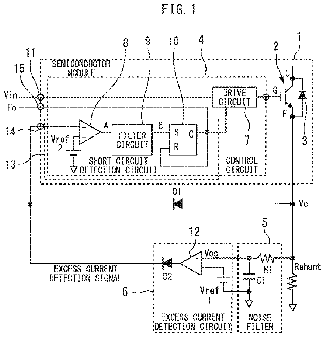
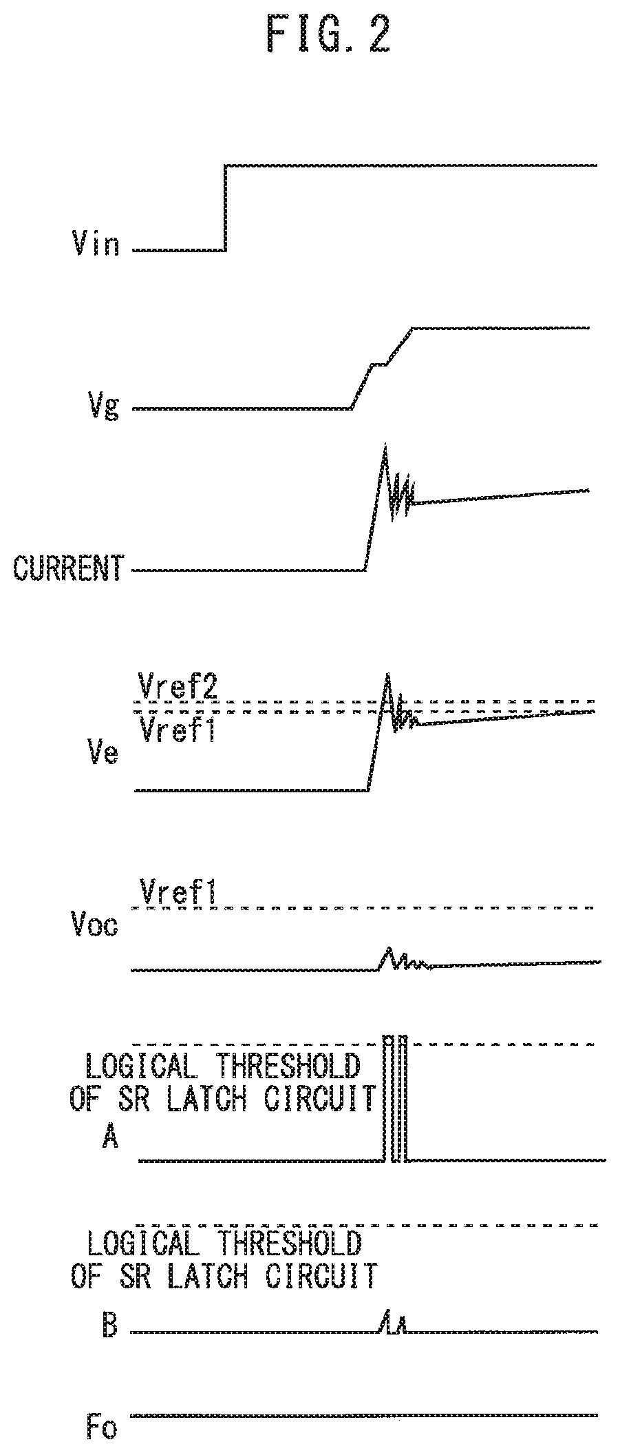
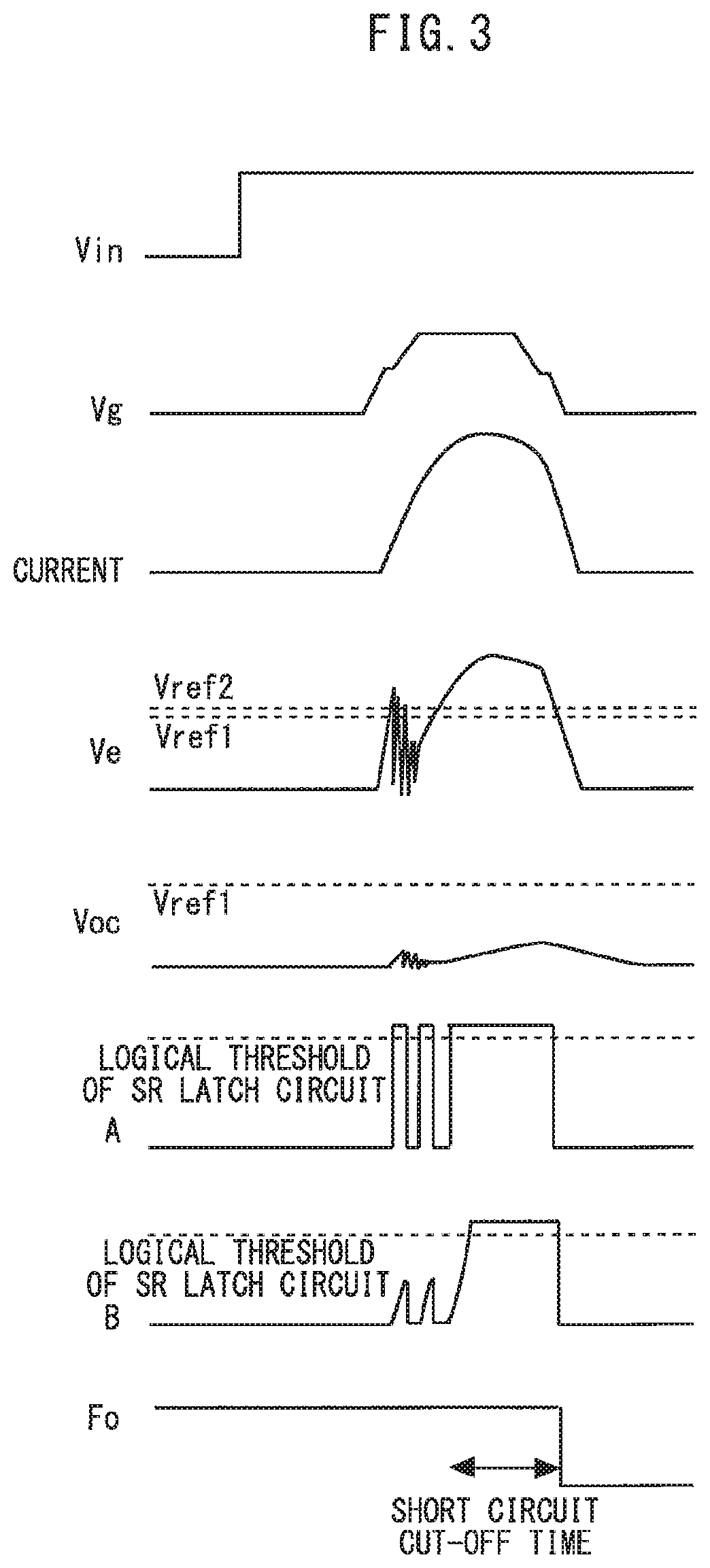
[0015]FIG. 1 is a diagram illustrating an inverter driver according to a first embodiment. A switching device 2, a free-wheel diode 3, and a control circuit 4 are provided in an interior of a semiconductor module 1. A shunt resistor Rshunt, a noise filter 5, an excess current detection circuit 6, and a diode D1 are provided in an exterior of the semiconductor module 1. The control circuit 4 includes a drive circuit 7, a comparator 8, a filter circuit 9, and an SR latch circuit 10.

[0016]The drive circuit 7 drives the switching device 2 according to an input voltage Vin input from an exterior into the semiconductor module 1 via a terminal 11. An IGBT is used as the switching device 2. The free-wheel diode 3 refluxes a current when the switching device 2 is off.

[0017]The shunt resistor Rshunt is connected between an emitter E of the switching device 2 and GND. The shunt resistor Rshunt constitutes a current detection device configured to generate a voltage signal Ve cor...

Example

Second Embodiment

[0027]FIG. 5 is a diagram illustrating an inverter driver according to a second embodiment. A terminal 17 is provided by which a negative terminal of a comparator 8 provided in an interior of a semiconductor module 1 is connected with a setting circuit 16 provided in an exterior of the semiconductor module 1. A second threshold value Vref2 is set to match a peak value of noise generated at the time of switching in the exterior of the semiconductor module 1 by the setting circuit 16. This can reduce further an erroneous detection of a short circuit.

Example

Third Embodiment

[0028]FIG. 6 is a diagram illustrating an inverter driver according to a third embodiment. A constant current circuit 18 is connected to a negative terminal of a comparator 8 and a terminal 17 in an interior of a semiconductor module 1. The constant current circuit 18 outputs a constant current Iscref. A resistor Rscref is connected between the terminal 17 and a GND in an exterior of the semiconductor module 1. A second threshold value Vref2 is set only based on a resistance value of the resistor Rscref in the exterior of the semiconductor module 1. This can reduce the size of the inverter driver in addition to the advantageous effect provided by the second embodiment.

[0029]The switching device 2 is not limited to a semiconductor device formed of silicon, but instead may be formed of a wide-bandgap semiconductor having a bandgap wider than that of silicon. The wide-bandgap semiconductor is, for example, a silicon carbide, a gallium-nitride-based material, or diamond....


PUM


Abstract

An inverter driver includes: a switching device; a drive circuit driving the switching device; a current detection device generating a voltage signal corresponding to a current flowing through the switching device; a noise filter removing noise superposed on the voltage signal; an excess current detection circuit outputting an excess current detection signal when the voltage signal input via the noise filter exceeds a first threshold value; and a short circuit detection circuit outputting an error signal when the excess current detection signal is input or the voltage signal input by bypassing the noise filter exceeds a second threshold value.

Description

BACKGROUND OF THE INVENTIONField[0001]The present invention relates to an inverter driver driving a switching device.Background[0002]In an inverter driver, a voltage signal corresponding to a current flowing through a switching device is input into a current detection circuit. The current detection circuit includes a comparator configured to detect an excess current and a comparator configured to detect a short circuit (for example, refer to JP 2017-212870 A).SUMMARY[0003]When a switching device is driven at a high speed, noise is superposed on a voltage signal, causing a short circuit or an excess current to be erroneously detected from time to time. A risk of occurrence of an erroneous detection due to noise is increased as the switching device is driven at faster speeds. A voltage signal thus needs to be input into a current detection circuit via a noise filter. However, since using the noise filter generates a certain delay time in detection, a switching device having a low shor...

Claims


Application Information

Patent Timeline
IPC IPC(8): H03K17/687H03K17/082H02M7/48H02M1/08
CPCH02M7/48H02M1/08H03K17/082H02M1/0009H02M1/32H03K17/0828
Inventor ODA, HISASHISAKAI, SHINJI
Owner MITSUBISHI ELECTRIC CORP
Why Eureka
Try Eureka