
Wide contact structure for small footprint radio frequency (RF) switch

a radio frequency switch and wide contact technology, applied in the field of semiconductor devices, can solve the problems of low operating voltage, large layout area of the rf switch, and inability to implement an rf switch, and achieve the effect of low resistance (and capacitance)

Active Publication Date: 2020-03-10
NEWPORT FAB
View PDF11 Cites 0 Cited by
  • Summary
  • Abstract
  • Description
  • Claims
  • Application Information

AI Technical Summary

Benefits of technology

The present invention provides a new structure for a MOS transistor used in a radio frequency (RF) switch. The transistor has a unique design with a plurality of source / drain regions and a plurality of polysilicon gate fingers. The design allows for a compact layout with a low on-resistance, making it ideal for use in an RF switch. The new structure also achieves a layout reduction of more than 15 percent compared to conventional structures.

Problems solved by technology

Note that transistors fabricated using more advanced process nodes (e.g., a 0.13 micron process node) have lower operating voltages (e.g., 1.2 Volts or lower), and are typically not suitable for implementing an RF switch.
As a result, the RF switch requires a significant layout area.

Method used


Image

  • Wide contact structure for small footprint radio frequency (RF) switch
  • Wide contact structure for small footprint radio frequency (RF) switch
  • Wide contact structure for small footprint radio frequency (RF) switch

Examples


Embodiment Construction

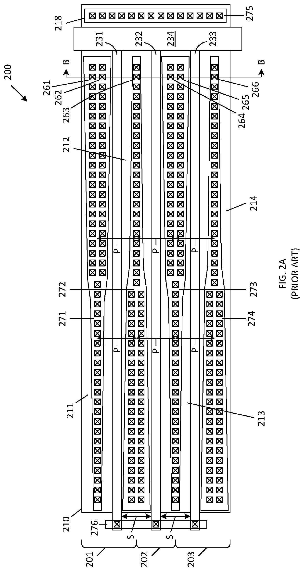
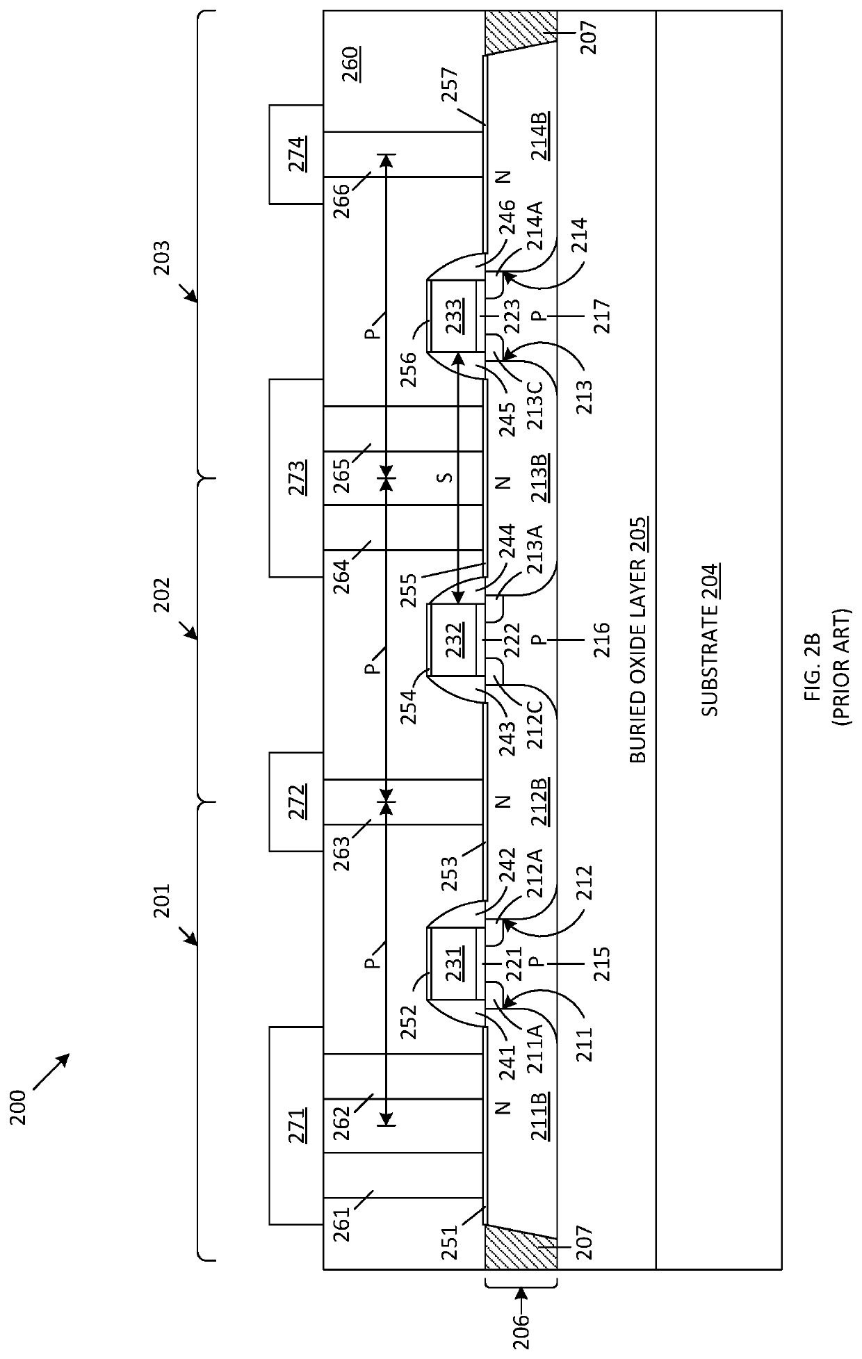
[0027]In general, the present invention includes an improved semiconductor structure for implementing a plurality of SOI CMOS transistors connected in series. In one embodiment, the series-connected SOI CMOS transistors are used to implement an RF switch. The SOI CMOS transistors are fabricated in accordance with a conventional SOI CMOS process node. In accordance with the present invention, the polysilicon gate fingers of the SOI CMOS transistors are ‘bent’ near a central location, in a manner that provides each source / drain region with both a narrow portion and a wide portion between adjacent polysilicon gate fingers. First sets of contacts, each including a first number of columns, are formed over the narrow portions of the source / drain regions, and second sets of contacts, each including a second number of columns (greater than the first number of columns), are formed over the wide portions of the source / drain regions. This configuration advantageously allows the pitch between a...


PUM


Abstract

A structure includes channel regions located between source / drain regions, and a polysilicon gate structure including a plurality of gate fingers, each extending over a corresponding channel region. Each gate finger includes first and second rectangular portions extending in parallel with a first axis, and a connector portion that introduces an offset between the first and second rectangular portions along a second axis. This offset causes each source / drain region to have a first section with a first length along the second axis, and a second section with a second length along the second axis, greater than the first length. A single column of contacts having a first width along the second axis is provided in the first section of each source / drain region, and a single column of contacts having a second width along the second axis, greater than the first width, is provided in the second section of each source / drain region.

Description

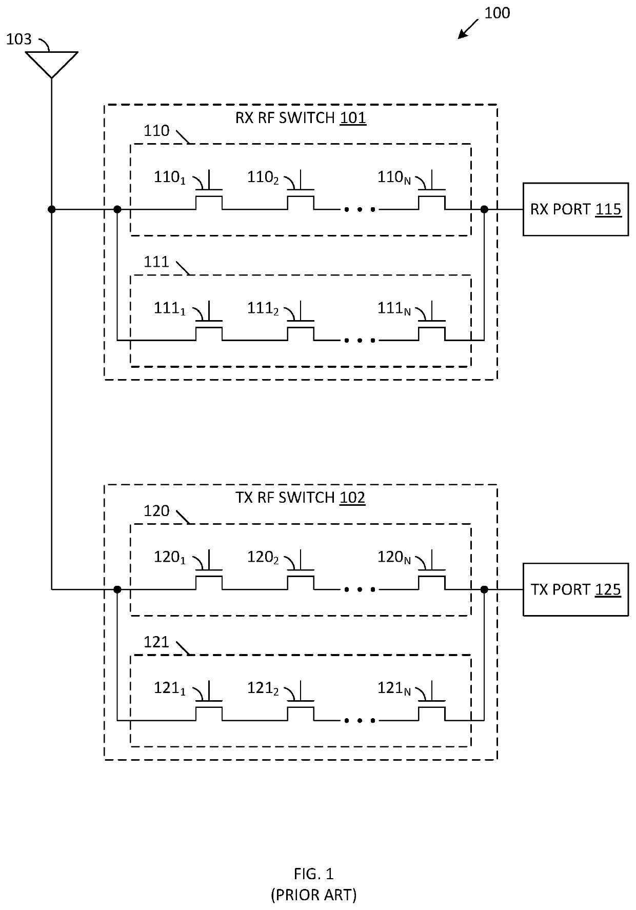
RELATED APPLICATIONS[0001]The present application is a continuation-in-part of U.S. patent application Ser. No. 15 / 900,112, “Bent Polysilicon Gate Structure For Small Footprint Radio Frequency (RF) Switch”, filed Feb. 20, 2018, by Roda Kanawati, Paul D. Hurwitz and Samir Chaudhry.FIELD OF THE INVENTION[0002]The present invention relates to a semiconductor structure including a plurality of series-connected silicon-on-insulator (SOI) CMOS transistors, which can be used to implement a radio frequency (RF) switch. More specifically, the present invention relates to the use of a wide contact structure for reducing the layout area required to implement an RF switch.RELATED ART[0003]FIG. 1 is a circuit diagram of a conventional radio frequency (RF) circuit 100, including an antenna 103, an RF receiver switch 101, an RF receiver port 115, an RF transmitter switch 102 and an RF transmitter port 125. RF receiver switch 101 includes a plurality of high-voltage field effect transistors (FETs) ...

Claims


Application Information

Patent Timeline
Patent Type & Authority Patents(United States)
IPC IPC(8): H01L29/00H01L29/78H01L29/786H01L29/06H01L29/423H01L29/49H01L29/66H01L29/10H01L23/482
CPCH01L29/0649H01L29/1095H01L29/66772H01L29/78615H01L23/4824H01L29/42376H01L29/783H01L29/4975H01L29/78654
Inventor KANAWATI, RODAHURWITZ, PAUL D.
Owner NEWPORT FAB
Learn More