

Wide contact structure for small footprint radio frequency (RF) switch
- Summary
- Abstract
- Description
- Claims
- Application Information
AI Technical Summary
Benefits of technology
Problems solved by technology
Method used
Image

Examples
Embodiment Construction
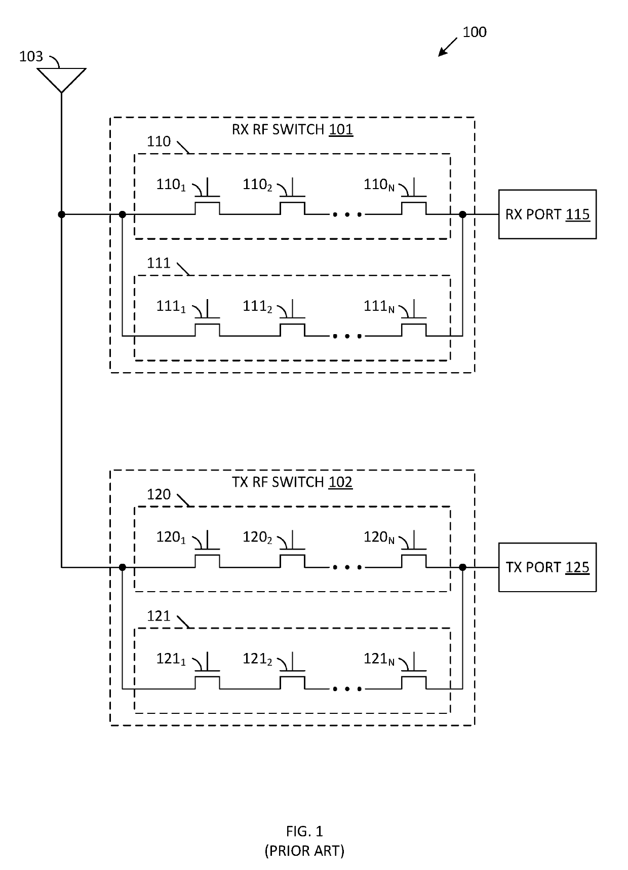
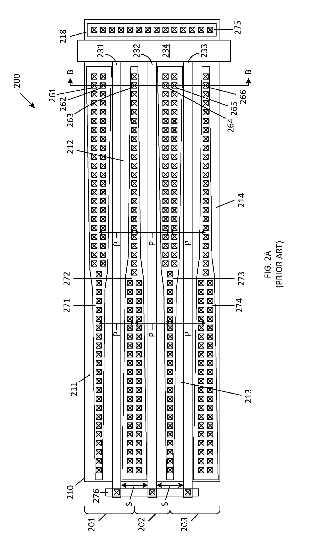
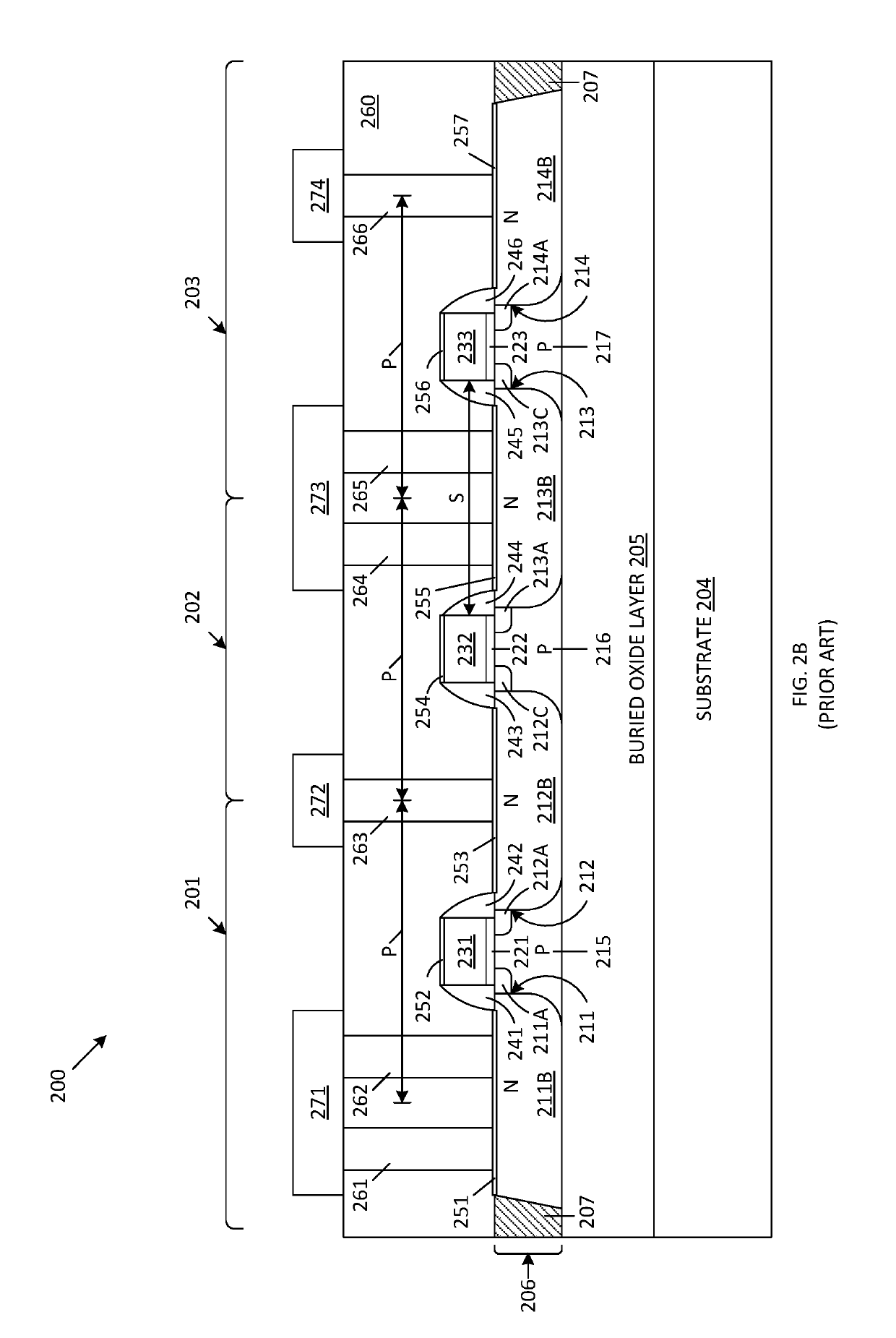
[0027]In general, the present invention includes an improved semiconductor structure for implementing a plurality of SOI CMOS transistors connected in series. In one embodiment, the series-connected SOI CMOS transistors are used to implement an RF switch. The SOI CMOS transistors are fabricated in accordance with a conventional SOI CMOS process node. In accordance with the present invention, the polysilicon gate fingers of the SOI CMOS transistors are ‘bent’ near a central location, in a manner that provides each source / drain region with both a narrow portion and a wide portion between adjacent polysilicon gate fingers. First sets of contacts, each including a first number of columns, are formed over the narrow portions of the source / drain regions, and second sets of contacts, each including a second number of columns (greater than the first number of columns), are formed over the wide portions of the source / drain regions. This configuration advantageously allows the pitch between a...
PUM
 Abstract
Description
Claims
Application Information