Manufacturing method of semiconductor device

a manufacturing method and semiconductor technology, applied in the direction of semiconductor devices, basic electric elements, electrical equipment, etc., can solve the problems of affecting the material properties of the material formed by epitaxial growth, the uniformity of electrical properties between different transistors may be worse, and the electrical performance of different transistors may be different from one another, so as to improve the uniformity of electrical properties of semiconductor devices.

Active Publication Date: 2020-03-31
UNITED MICROELECTRONICS CORP
View PDF19 Cites 0 Cited by
  • Summary
  • Abstract
  • Description
  • Claims
  • Application Information

AI Technical Summary

Benefits of technology

[0004]A manufacturing method of a semiconductor device is provided in the present invention. Ion implantations with different process conditions are performed to regions with different spacing distances between gate structures respectively for forming required doped regions. The difference between the influences from the ion implantations applied to the regions with different spacing distances between gate structures may be reduced, and the uniformity of the electrical properties of the semiconductor device may be improved accordingly.

Problems solved by technology

However, material properties of the materials formed by the epitaxial growth tend to be influenced by conditions of defects, such as stacking faults.
The electrical performance of the transistors may be different from one another when the distribution of the defects is not uniform.
The uniformity of the electrical properties between different transistors may become worse, and the manufacturing yield may be affected directly.

Method used


Image

  • Manufacturing method of semiconductor device
  • Manufacturing method of semiconductor device
  • Manufacturing method of semiconductor device

Examples


Embodiment Construction

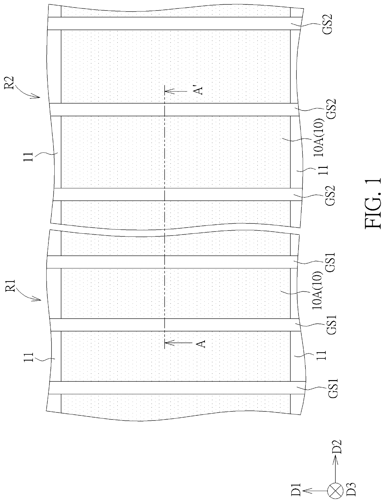
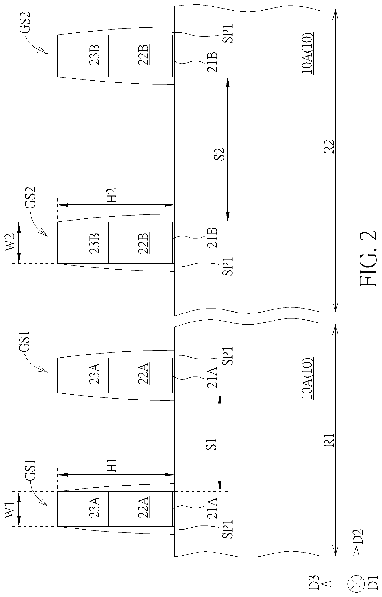
[0016]Please refer to FIGS. 1-6. FIGS. 1-6 are schematic drawings illustrating a manufacturing method of a semiconductor device according to a first embodiment of the present invention, wherein FIG. 1 is a top view diagram, and FIG. 2 may be regarded as a cross-sectional diagram taken along a line A-A′ in FIG. 1. The manufacturing method of the semiconductor device in this embodiment may include the following steps. As shown in FIG. 1 and FIG. 2, a semiconductor substrate 10 is provided, and the semiconductor substrate 10 includes a first region R1 and a second region R2 defined thereon. A plurality of first gate structures GS1 is formed on the first region R1 of the semiconductor substrate 10. A plurality of second gate structures GS2 is formed on the second region R2 of the semiconductor substrate 10. In some embodiments, each of the first gate structures GS1 and each of the second gate structures GS2 may extend in a first direction D1 respectively, the first gate structures GS1 m...


PUM

PropertyMeasurementUnit
widthaaaaaaaaaa
spacing distanceaaaaaaaaaa
tilt angleaaaaaaaaaa

Abstract

A manufacturing method of a semiconductor device includes following steps. First gate structures and second gate structures are formed on a first region and a second region of a semiconductor substrate respectively. A spacing distance between the second gate structures is larger than that between the first gate structures. A first ion implantation is preformed to form a first doped region between the first gate structures. A second ion implantation is performed to form a second doped region between the second gate structures. A tilt angle of the second ion implantation is larger than that of the first ion implantation. An implantation dose of the second ion implantation is lower than that of the first ion implantation. An etching process is performed to at least partially remove the first doped region to form a first recess and at least partially remove the second doped region to form a second recess.

Description

BACKGROUND OF THE INVENTION1. Field of the Invention[0001]The present invention relates to a manufacturing method of a semiconductor device, and more particularly, to a manufacturing method including an ion implantation.2. Description of the Prior Art[0002]With the development of technologies in the semiconductor integrated circuit industry, more and more semiconductor devices can be integrated in one semiconductor integrated circuit (IC), and the size of an individual semiconductor device becomes smaller and smaller. A field-effect transistor (FET) is a typical semiconductor device that constitutes a basic unit in a semiconductor IC. An FET includes a gate structure formed on a semiconductor substrate, as well as a source and a drain formed in the semiconductor substrate adjacent to the gate structure. Conventionally, the source and the drain are formed by doping the semiconductor substrate. With the integrity of the IC becomes higher and the FETs in the IC become smaller, differen...

Claims


Application Information

Patent Timeline
Patent Type & Authority Patents(United States)
IPC IPC(8): H01L29/66H01L27/02H01L21/336H01L21/265H01L21/266H01L21/8234H01L29/78H01L21/8238H01L21/306H01L21/84H01L21/3065
CPCH01L21/266H01L29/6656H01L29/7848H01L21/823431H01L21/26586H01L27/0207H01L21/823425H01L29/66636H01L21/823456H01L21/84H01L21/3065H01L21/30604H01L21/26506H01L21/823418
Inventor YEH, JIUN-LINTSENG, HSUEH-CHIHTSAI, CHIA-CHENLO, TA-KANG
Owner UNITED MICROELECTRONICS CORP
Why Eureka
Try Eureka