Method for production of semiconductor devices

a technology of semiconductor devices and production methods, applied in semiconductor/solid-state device manufacturing, basic electric elements, electric devices, etc., can solve the problem of extremely thin native oxide remaining after heat treatment, and achieve the effect of reducing gas, shortening time, and minimizing disadvantages

Inactive Publication Date: 2010-03-02
SONY CORP
View PDF13 Cites 1 Cited by
  • Summary
  • Abstract
  • Description
  • Claims
  • Application Information

AI Technical Summary

Benefits of technology

[0008]It is desirable to provide a method of removing native oxide, while protecting the wiring from oxidation, with a minimum damage to the interlayer insulating film by using in combination heat treatment with a reducing gas composed mainly of hydrogen and plasma treatment with a reducing gas.
[0009]The present invention is directed to a method for production of semiconductor devices which includes the steps of forming, on an interlayer insulating film formed on a substrate, a copper-containing conductive layer in such a way that its surface is exposed, performing heat treatment with a reducing gas composed mainly of hydrogen on the surface of the conductive layer. The method for production of semiconductor devices further includes the steps of performing plasma treatment with a reducing gas on the surface of the conductive layer, thereby permitting the surface of the conductive layer to be reduced and the hydrogen adsorbed by the heat treatment to be released, and forming an oxidation resistance film that covers the surface of the conductive layer such that the surface of the conductive layer is not exposed to an oxygen-containing atmospheric gas after the plasma treatment.
[0010]The method for production of semiconductor devices according to an embodiment of the present invention is intended to remove native oxide that has formed on the surface of a conductive layer. The native oxide is removed by performing heat treatment with a reducing gas composed mainly of hydrogen on the surface of a conductive layer and subsequently performing plasma treatment with a reducing gas. The advantage of the two-step method is that the heat treatment for reduction does not need such a large amount of heat as to damage the interlayer insulating film and the conductive layer. In other words, it is not necessary to completely remove native oxide by the heat treatment with a reducing gas composed mainly of hydrogen, because residual native oxide (if there is any) is removed by the subsequent plasma treatment for reduction. In the second step, the hydrogen which has been adsorbed by the heat treatment for reduction is released. Native oxide remaining after the heat treatment for reduction is extremely thin. Consequently, the plasma treatment with a reducing gas to completely remove residual native oxide can be accomplished in a very short time. The plasma treatment in this manner does not cause the low-dielectric insulating film to increase in dielectric constant or to recede. Thus, the method for production of semiconductor devices according to an embodiment of the present invention produces its effect by combination of heat treatment with a reducing gas composed mainly of hydrogen and plasma treatment with a reducing gas. The combination of two steps makes the best use of the advantages of individual steps, while minimizing their disadvantages.
[0011]The method for production of semiconductor devices according to an embodiment of the present invention involves heat treatment with a reducing gas composed mainly of hydrogen and plasma treatment with a reducing gas. The two steps combined together completely remove native oxide, without individual steps working harsh. Removal of native oxide in this manner prevents the interlayer insulating film from increasing in dielectric constant and from receding. In addition, plasma treatment with a reducing gas releases hydrogen which has entered the wiring or interlayer insulating film during heat treatment with a hydrogen-based reducing gas. This leads to a decrease in leakage current between wirings. The method of the present invention gives semiconductor devices with uniform electrical properties and high reliability.

Problems solved by technology

Native oxide remaining after the heat treatment for reduction is extremely thin.

Method used


Image

  • Method for production of semiconductor devices
  • Method for production of semiconductor devices
  • Method for production of semiconductor devices

Examples


Embodiment Construction

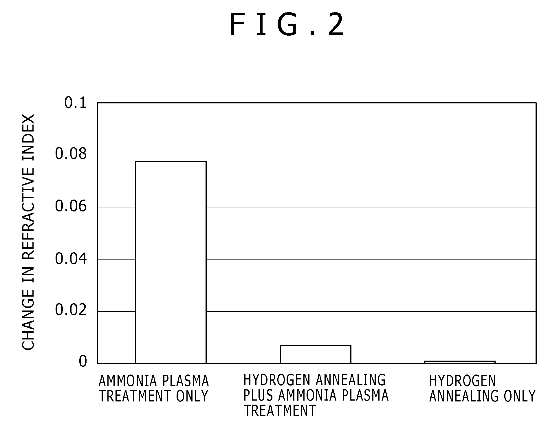
[0017]The method of the present invention is designed to remove native oxide from the surface of the conductive layer formed on a low-dielectric insulating layer by heat treatment with a hydrogen-based reducing gas and plasma treatment with a reducing gas which are performed successively. The combination of the two steps prevents the insulating film from increasing in dielectric constant and receding (detrimental to uniform electric properties and reliability) which would occur if the latter plasma treatment is performed alone.

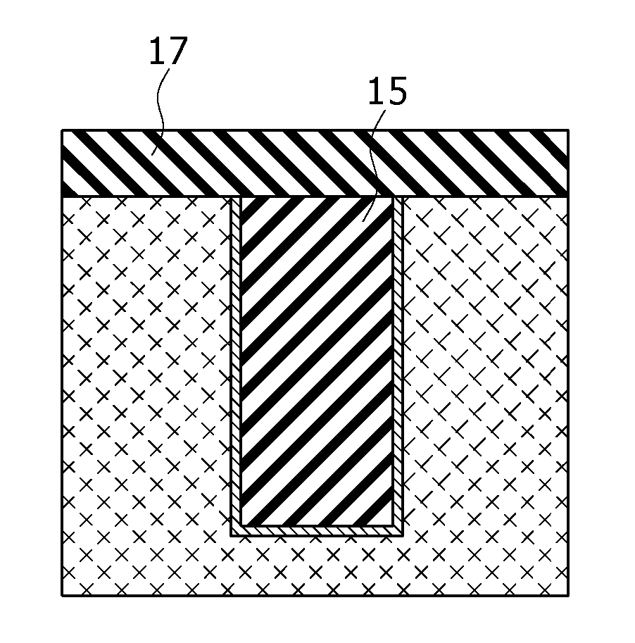
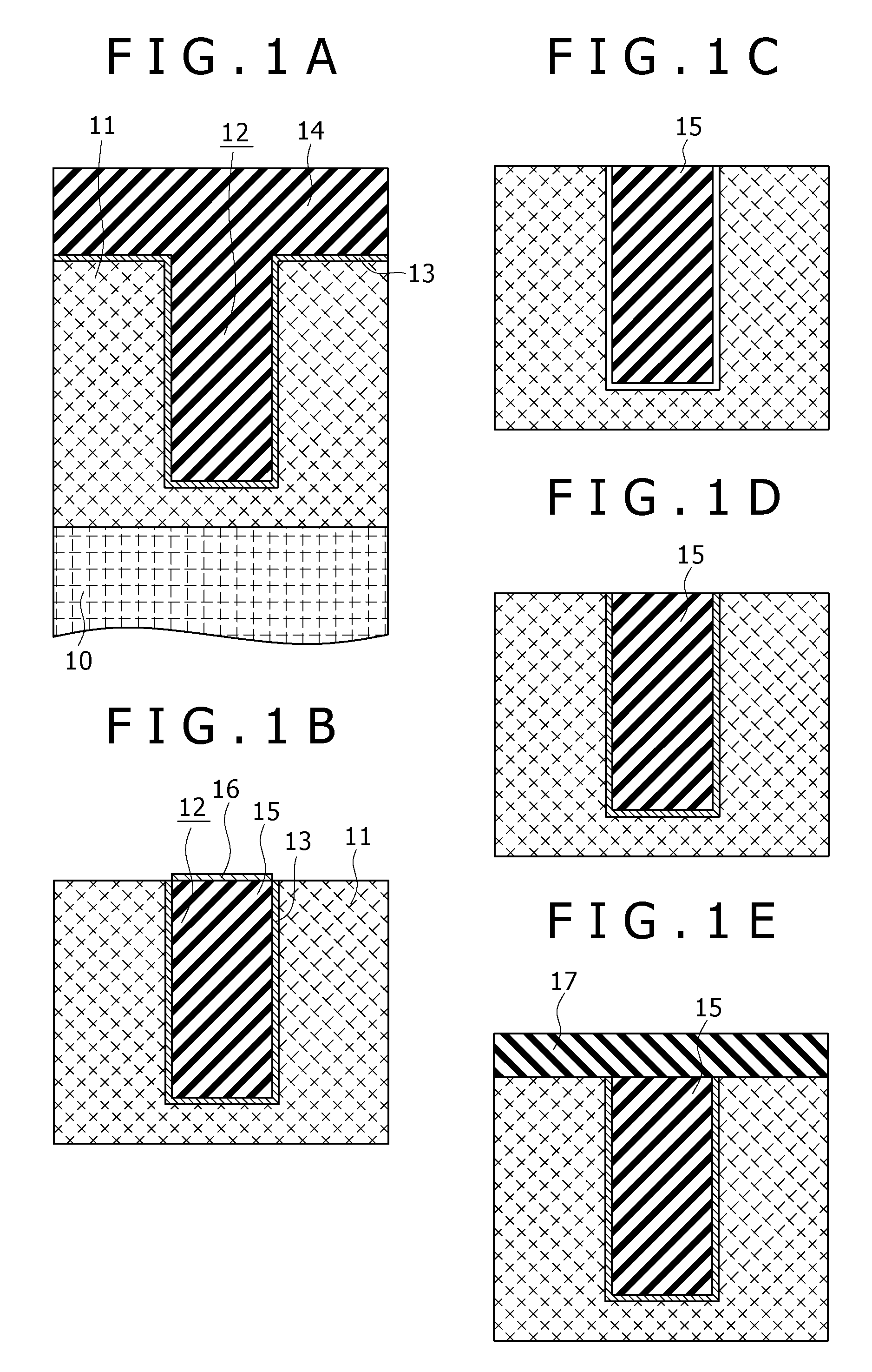
[0018]The method for production of semiconductor devices according to an embodiment of the present invention will be described with reference to one embodiment shown in FIG. 1, which is a schematic diagram not drawn to scale.

[0019]In FIG. 1A, there is shown a substrate 10, which is omitted in subsequent figures. First, a groove 12 for wiring is formed in an interlayer insulating film 11 on the substrate 10. The interlayer insulating film 11 may be a low-dielec...


PUM

PropertyMeasurementUnit
dielectric constantaaaaaaaaaa
thicknessaaaaaaaaaa
thicknessaaaaaaaaaa

Abstract

A method for production of semiconductor devices which includes the steps of forming, on an interlayer insulating film formed on a substrate, a copper-containing conductive layer in such a way that its surface is exposed, performing heat treatment with a reducing gas composed mainly of hydrogen on the surface of the conductive layer, performing plasma treatment with a reducing gas on the surface of the conductive layer, thereby permitting the surface of the conductive layer to be reduced and the hydrogen adsorbed by the heat treatment to be released, and forming an oxidation resistance film that covers the surface of the conductive layer such that the surface of the conductive layer is not exposed to an oxygen-containing atmospheric gas after the plasma treatment.

Description

CROSS REFERENCES TO RELATED APPLICATIONS[0001]The present invention contains subject matter related to Japanese Patent Application JP 2005-250614 filed in the Japanese Patent Office on Aug. 31, 2005, the entire contents of which being incorporated herein by reference.BACKGROUND OF THE INVENTION[0002]1. Field of the Invention[0003]The present invention relates to a method for production of semiconductor devices which permits easy removal of native oxide with a minimum damage to the substrate.[0004]2. Description of the Related Art[0005]Plasma treatment has been a common practice in the past technology. It alters the treated layer only slightly with very little adverse effect on reliability and working speed so long as it is performed on the wiring section of large area. However, this does not hold true any longer as the result of recent miniaturization of semiconductor devices, particularly in wiring. Reduced wiring width, increased current density, and multilayer structure require b...

Claims


Application Information

Patent Timeline
Patent Type & Authority Patents(United States)
IPC IPC(8): H01L21/00
CPCH01L21/02074H01L21/76877H01L21/76825H01L21/76826H01L21/76828H01L21/306
Inventor KAWANAMI, KOJITABUCHI, KIYOTAKA
Owner SONY CORP
Why Eureka
Try Eureka