Thin Film Transistor, Method of Manufacturing the Same, and Display Device Having Thin Film Transistor

a technology of thin film transistor and display device, which is applied in the direction of semiconductor devices, instruments, optics, etc., can solve the problems of image quality degradation, prevent the defect of inferior image quality of the display device caused by the malfunction, and minimize the leakage current and defect

Active Publication Date: 2011-09-15
SAMSUNG DISPLAY CO LTD
View PDF25 Cites 1 Cited by
  • Summary
  • Abstract
  • Description
  • Claims
  • Application Information

AI Technical Summary

Benefits of technology

[0008]Accordingly, embodiments of the present invention provide a thin film transistor capable of minimizing leakage current caused by electron holes, a method of manufacturing the same, and a display device including the thin film transistor.
[0015]According to the embodiments of the present invention, the semiconductor layer overlapped with the gate electrode includes 3.5 to 4.5 protrusions. When the number of protrusions is adjusted, as described above, in order to minimize the leakage current and the defect, the electrical property of the thin film transistor can be maintained uniform, and inferior image quality of the display device caused by the malfunction can be prevented.

Problems solved by technology

As a result, brightness is changed or there is a malfunction such as vertical crosstalk in which light is emitted in a vertical line form so that image quality is deteriorated.

Method used


Image

  • Thin Film Transistor, Method of Manufacturing the Same, and Display Device Having Thin Film Transistor
  • Thin Film Transistor, Method of Manufacturing the Same, and Display Device Having Thin Film Transistor
  • Thin Film Transistor, Method of Manufacturing the Same, and Display Device Having Thin Film Transistor

Examples


Embodiment Construction

[0027]In the following detailed description, only certain exemplary embodiments of the present invention have been shown and described, simply by way of illustration. As those skilled in the art will realize, the described embodiments may be modified in various different ways, all without departing from the spirit or scope of the present invention. Accordingly, the drawings and description are to be regarded as illustrative in nature and not restrictive. In addition, when an element is referred to as being “on” other element, it can be directly on the other element or be indirectly on the other element with one or more intervening elements interposed therebetween. Also, when an element is referred to as being “connected to” other element, it can be directly connected to the other element or be indirectly connected to the other element with one or more intervening elements interposed therebetween. Hereinafter, like reference numerals refer to like elements.

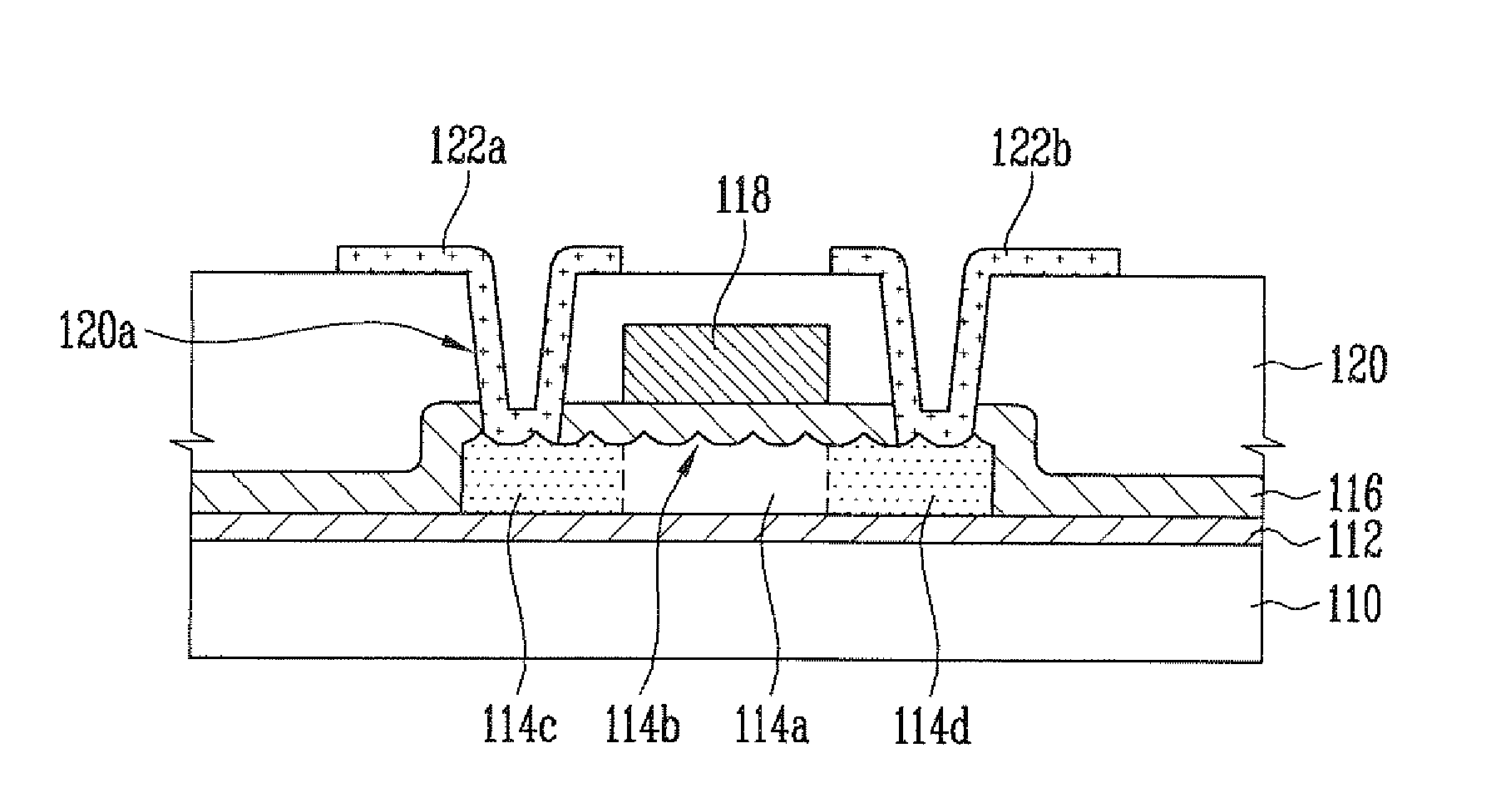
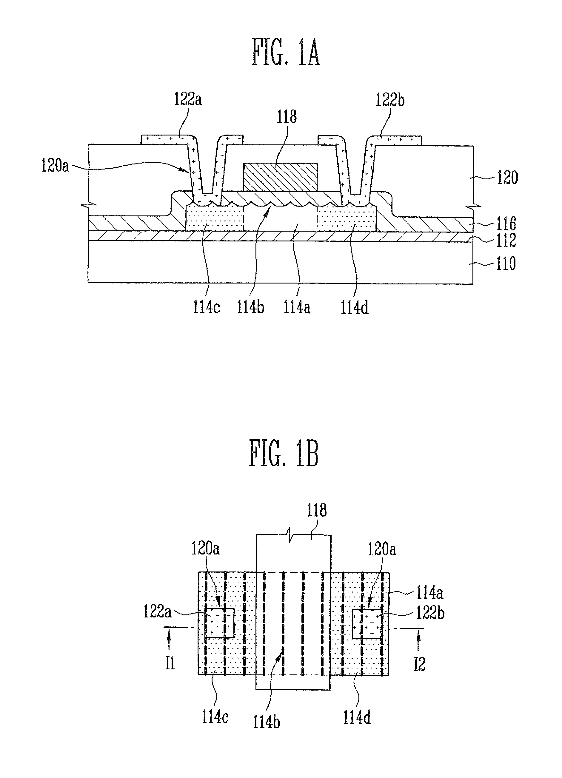
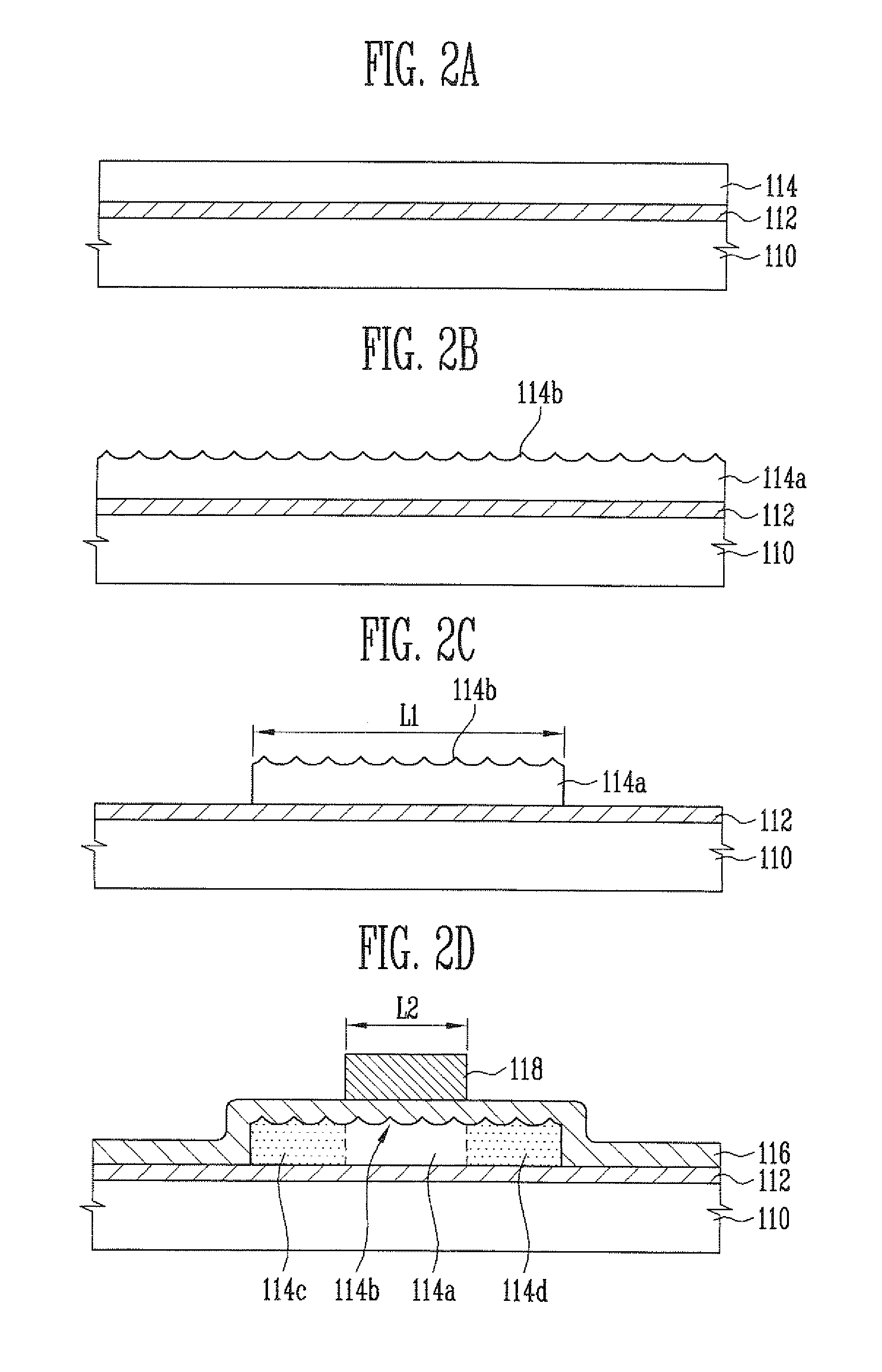
[0028]FIGS. 1A and 1B are a...


PUM

PropertyMeasurementUnit
length L2aaaaaaaaaa
length L2aaaaaaaaaa
brightnessaaaaaaaaaa

Abstract

A thin film transistor, a manufacturing method thereof, and a display device having the same are disclosed. The thin film transistor includes a semiconductor layer formed on a substrate, a gate insulating layer formed on the substrate including the semiconductor layer, a gate electrode formed on the gate insulating above the semiconductor layer, source and drain electrodes connected to the semiconductor layer, and 3.5 to 4.5 protrusions formed on the semiconductor layer overlapped with the gate electrode. Malfunction of the thin film transistor and inferior image quality of the display device can be prevented by adjusting the number of protrusions to minimize leakage current and defects.

Description

CLAIM OF PRIORITY[0001]This application makes reference to, incorporates the same herein, and claims all benefits accruing under 35 U.S.C. §119 from an application earlier filed in the Korean Intellectual Property Office on the 10 Mar. 2010 and there duly assigned Serial No. 10-2010-0021263.BACKGROUND OF THE INVENTION[0002]1. Field of the Invention[0003]The present invention relates to a thin film transistor, a method of manufacturing the same, and a display device having the thin film transistor and, more particularly, to a thin film transistor having a semiconductor layer formed by sequential lateral solidification (SLS), a method of manufacturing the same, and a display device having the thin film transistor.[0004]2. Description of the Related Art[0005]Liquid crystal display devices using the electro-optic property of a liquid crystal are classified into a passive matrix type and an active matrix type. The active matrix type liquid crystal display device using a thin film transis...

Claims


Application Information

Patent Timeline
Patent Type & Authority Applications(United States)
IPC IPC(8): G02F1/136H01L29/04H01L21/84
CPCH01L29/42384H01L29/66757H01L27/1285H01L29/78696H01L27/1214H01L29/78645H01L29/34
Inventor RO, SUNG-INPARK, JI-YONGPARK, KYUNG-MINPARK, JIN-SUKKANG, SEONG-YEUN
Owner SAMSUNG DISPLAY CO LTD
Why Eureka
Try Eureka