Semiconductor device and method of manufacturing the same

a semiconductor and capacitor technology, applied in semiconductor devices, capacitors, electrical devices, etc., can solve the problems of capacitor capacitance decline and leakage current increase, and achieve the effect of sufficient capacitance and minimal leakage curren

Active Publication Date: 2010-07-27
MICRON TECH INC
View PDF11 Cites 1 Cited by
  • Summary
  • Abstract
  • Description
  • Claims
  • Application Information

AI Technical Summary

Benefits of technology

[0007]An object of the present invention is to provide a semiconductor device having a capacitor structure capable of minimizing a leakage current with an amount of capacitance change smaller than ever before in a capacitor formed by using paraelectric films, and a method of manufacturing the semiconductor device.
[0032]According to the present invention, in a semiconductor device provided with a capacitor formed using paraelectric films, it is possible to minimize a leakage current with an amount of capacitance change smaller than ever before. Specifically, it is possible to provide a semiconductor device including a miniaturized capacitor wherein a sufficient capacitance is secured while suppressing a leakage current.

Problems solved by technology

However, simply thin-filming the dielectric film in an attempt to maintain the capacitance of the capacitor causes the leakage current thereof to increase.
Thickening the dielectric film in an attempt to prevent the increase of the leakage current results in the problem that the capacitor capacitance decreases.

Method used


Image

  • Semiconductor device and method of manufacturing the same
  • Semiconductor device and method of manufacturing the same
  • Semiconductor device and method of manufacturing the same

Examples


Embodiment Construction

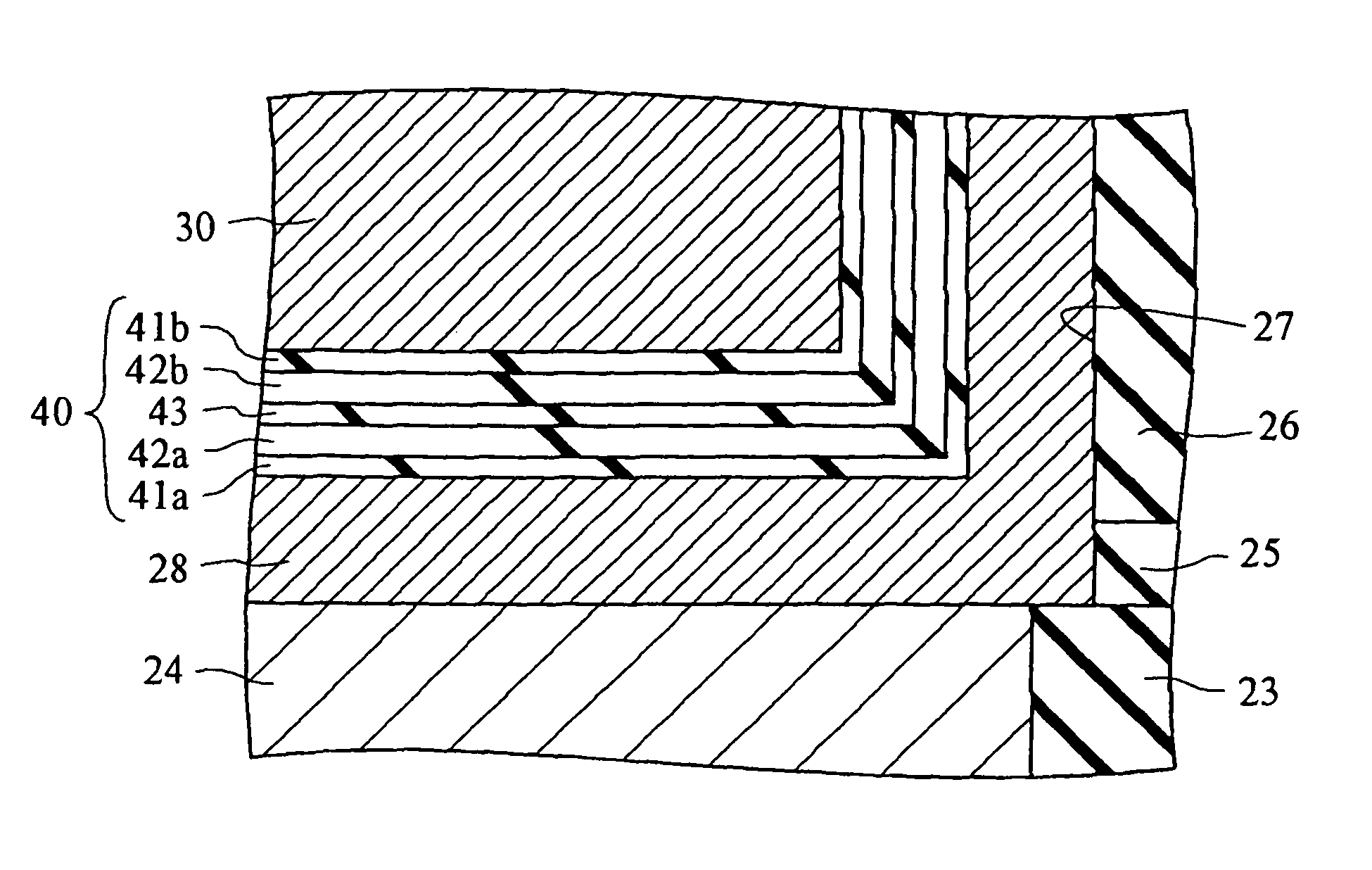
[0038]FIG. 1 is a cross-sectional view of the relevant part of a memory cell of a DRAM in accordance with the present exemplary embodiment. The DRAM of the present exemplary embodiment is formed on a semiconductor substrate wherein a plurality of active regions are divided off by element-isolating films formed of an insulating material, though not shown in the figure.

[0039]As shown in FIG. 1, the DRAM of the present exemplary embodiment includes two gate insulating films 11 crossing over the respective active regions of a silicon substrate 10. On each gate insulating film 11, there is formed a gate electrode 13a laminated with a polysilicon layer 12a and a tungsten layer 12b. The two gate electrodes 13a form part of word lines provided in parallel so as to linearly extend over the silicon substrate 10 across the plurality of active regions. In addition, dummy gate electrodes 13b are formed so as to sandwich the two gate electrode 13a.

[0040]A cap insulating layer 14 formed of silico...


PUM

PropertyMeasurementUnit
inner diameteraaaaaaaaaa
thicknessaaaaaaaaaa
breakdown voltageaaaaaaaaaa

Abstract

A semiconductor device including a capacitor which includes a first electrode, a second electrode, and a dielectric layer disposed between the first electrode and the second electrode, the dielectric layer including: a first paraelectric film formed of a material containing a first metal element and at least one kind of second metal element; a second paraelectric film disposed between the first electrode and the first paraelectric film; and a third paraelectric film disposed between the second electrode and the first paraelectric film, wherein the second paraelectric film is formed of a material containing the first metal element but substantially not containing the second metal element, and the third paraelectric film is formed of a material containing the first metal element but substantially not containing the second metal element.

Description

BACKGROUND OF THE INVENTION[0001]1. Field of the Invention[0002]The present invention relates to a semiconductor device and, more particularly, to a semiconductor device provided with a capacitor formed by holding a paraelectric film between electrodes and to a method of manufacturing the semiconductor device.[0003]2. Description of the Related Art[0004]In semiconductor devices, including a dynamic random access memory (DRAM), elements are required to be integrated at a high density. As a result, a capacitor composing a memory cell is also required to be downsized. Capacitors of a conventional DRAM are formed by, for example, holding a dielectric film, such as a silicon nitride (SiN) film or a tantalum oxide (TaO) film, between conductor films, such as titanium nitride (TiN) films.[0005]The capacitance of a capacitor have to be maintained while downsizing the capacitor. However, simply thin-filming the dielectric film in an attempt to maintain the capacitance of the capacitor causes...

Claims


Application Information

Patent Timeline
Patent Type & Authority Patents(United States)
IPC IPC(8): H01L27/108
CPCH01L28/65H01L28/91H01L27/10817H01L27/1085H10B12/318H10B12/03
Inventor TANIOKU, MASAMI
Owner MICRON TECH INC
Why Eureka
Try Eureka