Thin film transistor, method of manufacturing the thin film transistor and organic light emitting display device having the thin film transistor

a technology of thin film transistor and organic light, which is applied in the direction of basic electric elements, semiconductor devices, electrical equipment, etc., can solve the problems of high mobility, uneven threshold voltage, and difficulty in implementing a drive circuit operated at a high speed, and achieve the effect of improving electrical characteristics

Active Publication Date: 2011-04-28
SAMSUNG DISPLAY CO LTD
View PDF2 Cites 1 Cited by
  • Summary
  • Abstract
  • Description
  • Claims
  • Application Information

AI Technical Summary

Benefits of technology

[0012]In one embodiment of the present invention, there are provided a thin film transistor (TFT) using an oxide semiconductor as an active layer and having improved electrical characteristics, a method of manufacturing the TFT and an organic light emitting display device having the TFT.

Problems solved by technology

However, if the active layer is formed of amorphous silicon, mobility is low, and therefore, it is difficult to implement a drive circuit operated at a high speed.
If the active layer is formed of poly-silicon, the mobility is high, but threshold voltage is uneven.
In a related art method of manufacturing a TFT using a low temperature poly-silicon (LTPS), a high-priced process such as laser heat treatment is performed, and it is difficult to control characteristics of the TFT.
Therefore, it is difficult to apply the related art method to large-area substrates.
Therefore, the structure of the related art TFT has difficulty implementing electrical characteristics necessary for a pixel drive circuit of a display device or a peripheral circuit.

Method used


Image

  • Thin film transistor, method of manufacturing the thin film transistor and organic light emitting display device having the thin film transistor
  • Thin film transistor, method of manufacturing the thin film transistor and organic light emitting display device having the thin film transistor
  • Thin film transistor, method of manufacturing the thin film transistor and organic light emitting display device having the thin film transistor

Examples


Embodiment Construction

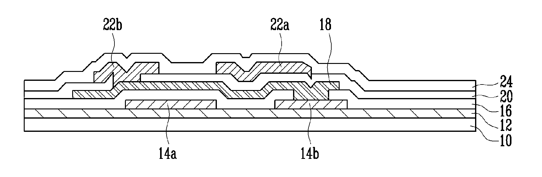
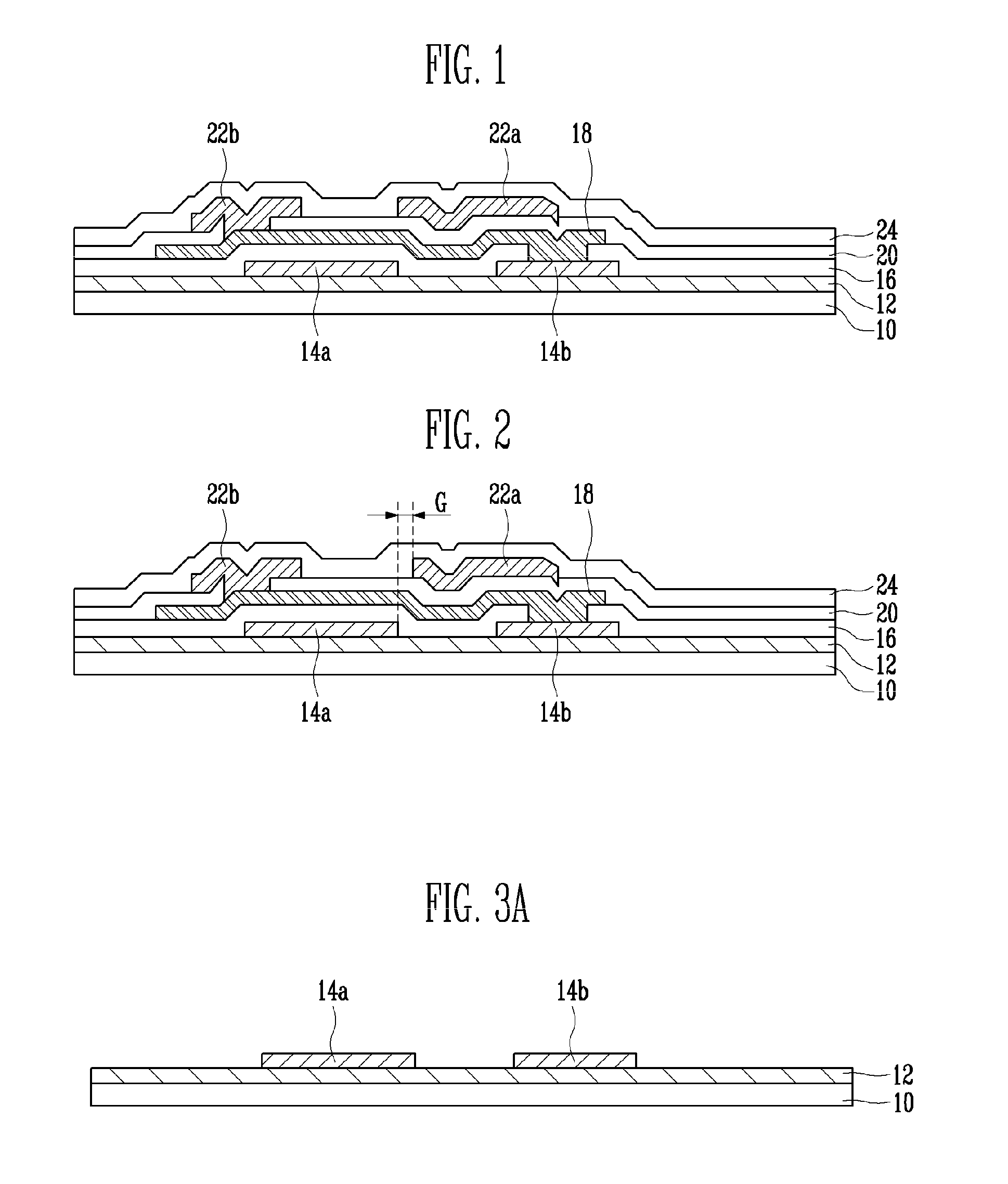
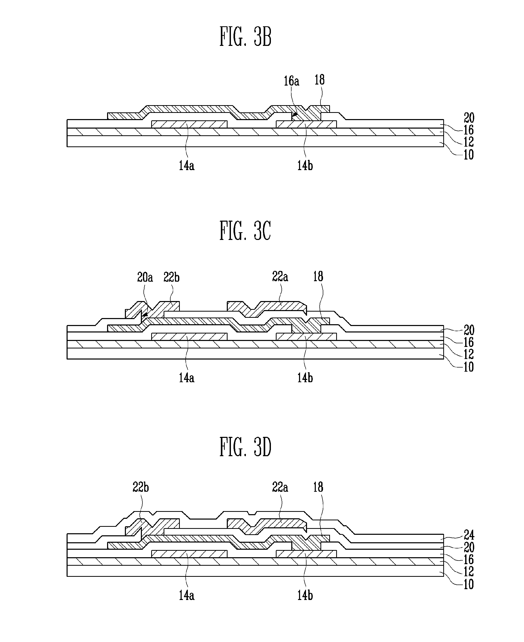
[0027]Reference will now be made in detail to the present embodiments of the present invention, examples of which are illustrated in the accompanying drawings, wherein like reference numerals refer to the like elements throughout. The embodiments are described below in order to explain the present invention by referring to the figures.

[0028]In the following detailed description, only certain exemplary embodiments of the present invention have been shown and described, simply by way of illustration. As those skilled in the art would realize, the described embodiments may be modified in various different ways, all without departing from the spirit or scope of the present invention. Accordingly, the drawings and description are to be regarded as illustrative in nature and not restrictive. In addition, when an element is referred to as being “on” another element, it can be directly on the other element or be indirectly on the other element with one or more intervening elements interpose...


PUM


Abstract

A thin film transistor (TFT) using an oxide semiconductor as an active layer, a method of manufacturing the TFT and an organic light emitting display device having the TFT. In one embodiment, a TFT includes a first gate electrode formed on a substrate. A source electrode is formed to be spaced apart from the gate electrode on the substrate. A first insulating layer is formed on the substrate. An active layer is formed of an oxide semiconductor on the first insulating layer, and connected to the source electrode. A second insulating layer is formed on the first insulating layer. A second gate electrode is formed on the second insulating layer so as not to overlap with the first gate electrode. A drain electrode is formed to be spaced apart from the second gate electrode on the second insulating layer, and connected to the active layer.

Description

CROSS-REFERENCE TO RELATED APPLICATION[0001]This application claims the benefit of Korean Patent Application No. 10-2009-0102277, filed on Oct. 27, 2009, in the Korean Intellectual Property Office, the disclosure of which is incorporated herein by reference.BACKGROUND[0002]1. Field[0003]An aspect of the present invention relates to a thin film transistor (TFT) using an oxide semiconductor as an active layer, a method of manufacturing the TFT and an organic light emitting display device having the TFT. More particularly, an aspect of the present invention relates to a TFT having two gate electrodes disposed into a non-symmetric structure, a method of manufacturing the TFT and an organic light emitting display device having the TFT.[0004]2. Description of the Related Art[0005]In general, a thin film transistor (TFT) includes an active layer and a gate electrode. Here, the active layer provides channel, source and drain regions. The gate electrode overlaps with the channel region and i...

Claims


Application Information

Patent Timeline
Patent Type & Authority Applications(United States)
IPC IPC(8): H01L29/12H01L21/16
CPCH01L29/7869H01L27/1225H01L21/02148H01L21/02159H01L31/022475H01L31/022483
Inventor KIM, KI-WOOK
Owner SAMSUNG DISPLAY CO LTD
Why Eureka
Try Eureka