Oscillator arrangement for time-to-digital converter for large array of time-of-flight image sensor devices

a time-to-digital converter and image sensor technology, applied in the field of integrated time-of-flight image sensor devices, can solve the problems of large quantization noise, difficult calibration of dynamic variations, limited reference phase/frequency of time-to-digital converters over a large sensor pixel area, etc., and achieve stable well-defined frequency and reduce calibration requirements

Active Publication Date: 2020-04-28
ECOLE POLYTECHNIQUE FEDERALE DE LAUSANNE (EPFL)
View PDF1 Cites 1 Cited by
  • Summary
  • Abstract
  • Description
  • Claims
  • Application Information

AI Technical Summary

Benefits of technology

[0014]In general, providing an accurate reference phase / frequency for time-to-digital converters over a large sensor pixel area is limited by physical constraints depending on silicon imperfections, manufacturability variations, temperature IR drop, circuit asymmetries and the like. While some of the static variabilities can be compensated for, dynamic variations are hard to calibrate. Moreover, for long-term measurements, the accumulated jitter may cause larger imprecision than the quantization noise itself. Thus, a coherent design of the time-to-digital converter considering the jitter and resolution is needed. A finer time-to-digital converter resolution, which can lead to higher power consumption and data, is only justifiable if its correspondent jitter matches the quantization noise.
[0015]The above oscillator arrangement provides an oscillator grid which is at least partly spread over the sensor pixel area to provide timing information to time-to-digital converters each used by a portion of the pixels of the sensor pixel area. The time-to-digital converters are each associated to one of the oscillators of the oscillator arrangement which are mutually coupled with at least one oscillator of a neighbored time-to-digital converter. Such an arrangement overcomes the need for a centralized frequency generation and distribution.
[0017]Above oscillator arrangement for time-to-digital converters achieve a robust synchronization of timing signals supplied by the ring oscillators while further greatly reducing the phase noise which is at about the same frequency uncorrelated in different oscillators. Furthermore, it provides a low process-voltage-temperature dependency and similar power consumption of the sum of the number of oscillators, without extra power being spent in the synchronization.
[0024]Moreover, a PLL circuit may be provided which controls the oscillators depending on a reference frequency signal to adjust the frequency to a provided reference frequency. The PLL circuit may be an analog PLL circuit and configured to provide a common control voltage depending on one of the oscillators phases with respect to the reference frequency to control all oscillators. Alternatively, the PLL circuit may be a digital PLL (or digital word, in case of a digital PLL), shared among the oscillator, By implementing a single global PLL circuit slow temperature drifts can be tracked and compensated and a stable well-defined frequency can be provided, thereby reducing calibration requirements.

Problems solved by technology

In general, providing an accurate reference phase / frequency for time-to-digital converters over a large sensor pixel area is limited by physical constraints depending on silicon imperfections, manufacturability variations, temperature IR drop, circuit asymmetries and the like.
While some of the static variabilities can be compensated for, dynamic variations are hard to calibrate.
Moreover, for long-term measurements, the accumulated jitter may cause larger imprecision than the quantization noise itself.
A finer time-to-digital converter resolution, which can lead to higher power consumption and data, is only justifiable if its correspondent jitter matches the quantization noise.

Method used


Image

  • Oscillator arrangement for time-to-digital converter for large array of time-of-flight image sensor devices
  • Oscillator arrangement for time-to-digital converter for large array of time-of-flight image sensor devices
  • Oscillator arrangement for time-to-digital converter for large array of time-of-flight image sensor devices

Examples


Embodiment Construction

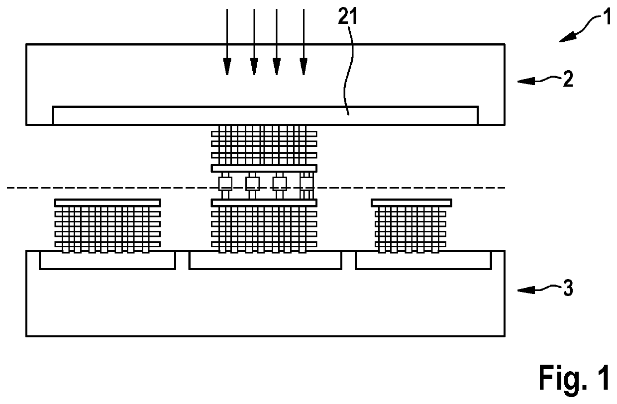
[0037]In the following, a basic structure of a 3D image sensor device of one embodiment is described in detail. Such an exemplary 3D image sensor device 1 is shown in FIG. 1 in a cross-sectional view. Substantially, the 3D image sensor device 1 has a stacked configuration with a sensing layer 2 including the pixel sensors in an array 21 formed with one avalanche photodiodes operating in Geiger mode, also known as single photon avalanche diodes SPAD, per pixel.

[0038]In a detection layer 3, a read-out circuitry 31 is coupled with the photodiode array 21. The read-out circuitry 31 is implemented including time-to-digital converters, each associated to one or more of the pixels included in the sensing layer 2. Particularly, the time-to-digital converters each are associated to the pixels (photodiodes) of a portion of the pixel area, substantially a rectangular area portion. To reduce signal propagation delays, the time-to-digital converters are directly arranged under the respective pix...


PUM


Abstract

An oscillator arrangement for time-to-digital converters for a 3D image sensor device includes a plurality of oscillators arranged as an array each oscillator being associated to one time-to-digital converter, and at least one coupling unit respectively arranged between at least two of the oscillators, so that oscillation in the at least two oscillators at a fundamental frequency is synchronized between the at least two coupled oscillators.

Description

TECHNICAL FIELD[0001]The present invention relates to integrated time-of-flight image sensor devices for 3D imaging applications.TECHNICAL BACKGROUND[0002]Time-resolved optical sensors have become important for various applications, such as PET, FLEM and LiDAR. These image sensor devices, when implemented in CMOS, generally comprise avalanche photodiodes operating in Geiger mode, known as single photon avalanche diodes (SPAD), and time-to-digital converters which determine the time of arrival of photons. The photodiodes are arranged in an array of a sensor pixel area. One or more photodiodes are each coupled with one time-to-digital converter, so that in time-correlated operation mode, the timing of incoming photons which are periodically generated by a laser can be precisely measured so that an accurate 3D image reconstruction of the scanned scene can be obtained.[0003]Time-of-flight image sensors require high levels of accuracy and precision on time quantization typically using ti...

Claims


Application Information

Patent Timeline
Patent Type & Authority Patents(United States)
IPC IPC(8): G01S7/486H03L7/099G04F10/00G01S7/4865G01S17/89H03H7/38
CPCG01S7/4865G01S17/89H03L7/0995G04F10/005H03H7/38
Inventor RONCHINI XIMENES, AUGUSTOPADMANABHAN, PREETHICHARBON, EDOARDO
Owner ECOLE POLYTECHNIQUE FEDERALE DE LAUSANNE (EPFL)
Why Eureka
Try Eureka