
Compound semiconductor device and production method for the same

a semiconductor and production method technology, applied in the direction of semiconductor devices, basic electric elements, electrical appliances, etc., can solve the problems of increased jfet portion, increased on-resistance, high electric field strength at off-time, etc., to achieve the effect of increasing on-resistance and increasing electric field strength

Active Publication Date: 2020-05-05
DENSO CORP
View PDF9 Cites 0 Cited by
  • Summary
  • Abstract
  • Description
  • Claims
  • Application Information

AI Technical Summary

Benefits of technology

This patent text describes a new method for making compound semiconductor devices. The method reduces the resistance of the device and prevents it from breaking down more easily. This is achieved by creating a specific structure at the bottom of the device, which minimizes the electric field concentration and prevents it from increasing during use. This structure also allows for a thinner deep layer, which is important for maintaining performance and reducing on-resistance.

Problems solved by technology

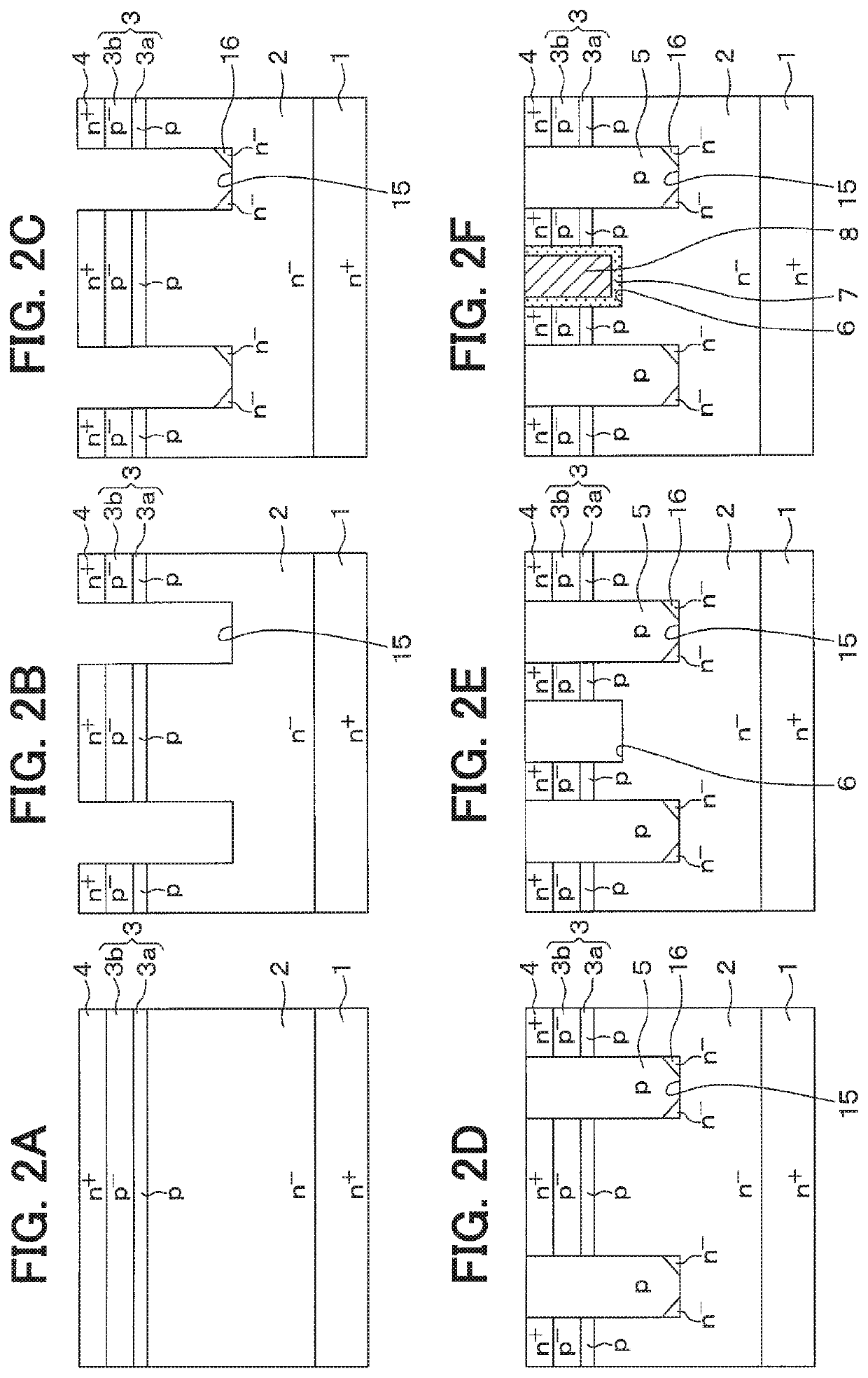
However, when the p-type deep layer is formed in the deep trench at a uniform concentration by epitaxial growth, because a corner portion at a bottom of the deep trench is pointed, an electric field strength at off-time is high at the corner portion, and a deterioration in the breakdown voltage is caused.
Also in such a case, when the deep layer is made deeper, an issue that a JFET portion increases and an on-resistance increases may be caused similarly to the above-described case.

Method used


Image

  • Compound semiconductor device and production method for the same
  • Compound semiconductor device and production method for the same
  • Compound semiconductor device and production method for the same

Examples


first embodiment

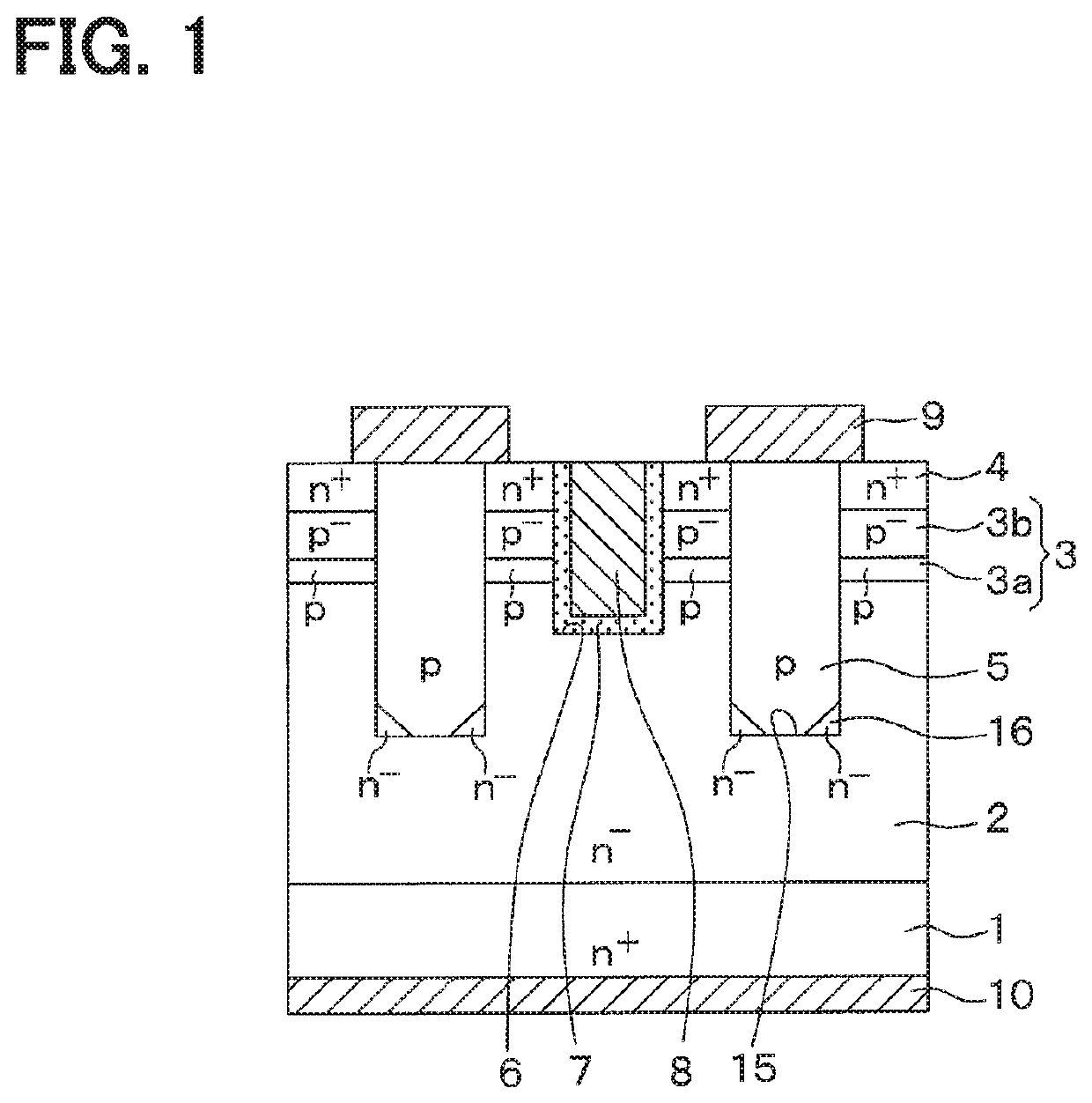
[0021]A SiC semiconductor device according to a first embodiment of the present disclosure in which an inverted vertical MOSFET having a trench gate structure is formed will be described with reference to FIG. 1.

[0022]In the SiC semiconductor device shown in FIG. 1, the vertical MOSFET having the trench gate structure is formed in a cell region, and an outer peripheral high breakdown voltage structure is formed in an outer peripheral region surrounding the cell region.

[0023]The SiC semiconductor device is formed using a semiconductor substrate in which an n−-type drift layer 2 made of SiC having a lower impurity concentration than an n+-type substrate 1 is formed on a front surface side of the n+-type substrate 1 that forms a high concentration impurity layer made of SiC. The n+-type substrate 1 has an n-type impurity concentration of, for example, 1.0×10¹⁹ / cm3 and a front surface of the n+-type substrate 1 is (0001) Si plane. The n−-type drift layer 2 has an n-type impurity concent...

second embodiment

Modification of Second Embodiment

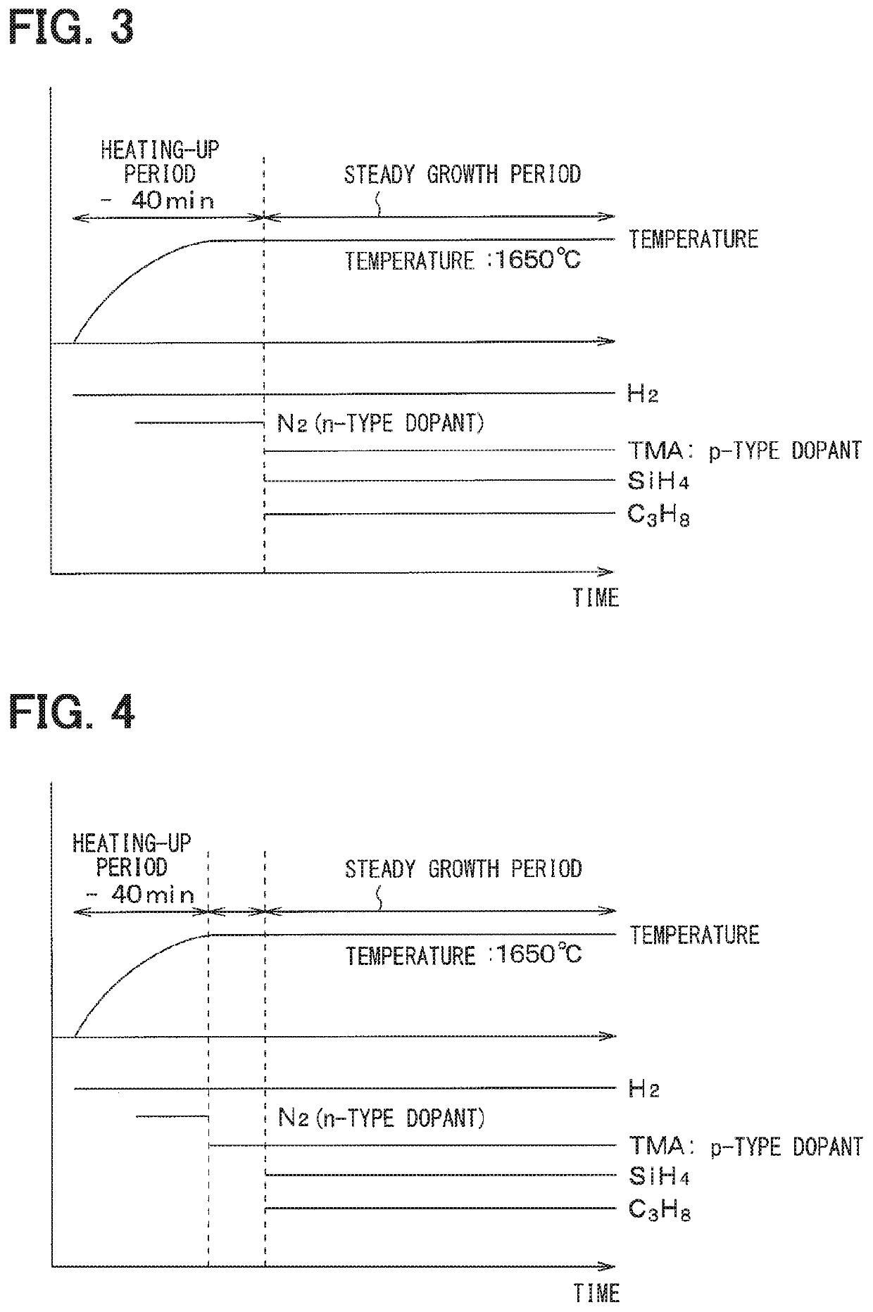
[0062]In the above-described second embodiment, the switching of the dopant gases is performed before the introduction of the SiC source gas. On the contrary, as shown in FIG. 5, the switching of the dopant gases can also be performed after the introduction of the SiC source gas. Accordingly, the p-type deep layer 5 can be formed later, and the range where the n−-type region 16 is formed can be expanded.

third embodiment

[0063]A third embodiment will be described. In the present embodiment, a configuration of the p-type deep layer 5 is changed with respect to the first embodiment, and others are similar to the first embodiment. Thus, only portions different from the first embodiment will be described.

[0064]As shown in FIG. 6, in the vertical MOSFET provided in the SiC semiconductor device according to the present embodiment, the p-type deep layer 5 has two-layer structure in which the p-type deep layer 5 described in the first embodiment is set as an upper p-type deep layer 5a, and a lower p-type deep layer 5b is provided below the upper p-type deep layer 5a and the n−-type region 16. The lower p-type deep layer 5b is connected with the upper p-type deep layer 5a, and the upper p-type deep layer 5a and the lower p-type deep layer 5b are set to the source potential. A corner portion on a bottom of the lower p-type deep layer 5b has a rounded shape.

[0065]In this way, the p-type deep layer 5b may be re...


PUM

PropertyMeasurementUnit
thicknessaaaaaaaaaa
thicknessaaaaaaaaaa
aspect ratioaaaaaaaaaa

Abstract

A compound semiconductor device includes a semiconductor substrate having a ground layer of a first conductivity type made of a compound semiconductor, a first conductivity type region formed at a corner portion of a bottom of a deep trench formed to the ground layer, and a deep layer of a second conductivity type formed in the deep trench so as to cover the first conductivity type region. A cross section of the first conductivity type region is a triangular shape or a rounded triangular shape in which a portion of the first conductivity type region being in contact with the deep layer is recessed to have a curved surface.

Description

CROSS REFERENCE TO RELATED APPLICATIONS[0001]This application is a U.S. national phase of International Application No. PCT / JP2017 / 000799 filed on Jan. 12, 2017, and is based on Japanese Patent Application No. 2016-32292 filed on Feb. 23, 2016, the disclosure of which is incorporated herein by reference.TECHNICAL FIELD[0002]The present disclosure relates to a compound semiconductor device using a compound semiconductor such as silicon carbide (hereafter referred to as SiC) and gallium nitride (hereafter referred to as GaN), and a production method for the same.BACKGROUND ART[0003]Conventionally, Patent Literature 1 proposes a SiC semiconductor device that includes a vertical MOSFET having an inverted trench gate structure as a vertical switching element having a trench gate structure. In the vertical MOSFET having the inverted trench gate structure, a gate voltage is applied to a gate electrode in a gate trench so that a channel is formed in a p-type base region located on a sidewal...

Claims


Application Information

Patent Timeline
Patent Type & Authority Patents(United States)
IPC IPC(8): H01L29/78H01L21/266H01L21/02H01L29/10H01L29/66H01L29/06H01L29/16H01L29/20H01L29/423H01L29/872
CPCH01L29/0619H01L29/66734H01L21/266H01L21/02576H01L29/66068H01L29/872H01L21/0262H01L29/6606H01L29/7813H01L21/02378H01L21/02529H01L21/02639H01L29/1608H01L29/4236H01L29/2003H01L29/1095H01L21/0243
Inventor TAKEUCHI, YUICHIAKIBA, ATSUYASUZUKI, KATSUMIAOI, SACHIKO
Owner DENSO CORP
Learn More