Compound semiconductor device and production method for the same

Active Publication Date: 2019-01-17
DENSO CORP
View PDF2 Cites 4 Cited by
  • Summary
  • Abstract
  • Description
  • Claims
  • Application Information

AI Technical Summary

Benefits of technology

The present invention provides a method to make a semiconductor device that can reduce its resistance and prevent breakdown. This is achieved by forming a region with a specific shape at the bottom of a deep layer, which helps to reduce the electric field concentration and maintain the breakdown voltage. This design helps to improve the device's performance by reducing its on-resistance.

Problems solved by technology

However, when the p-type deep layer is formed in the deep trench at a uniform concentration by epitaxial growth, because a corner portion at a bottom of the deep trench is pointed, an electric field strength at off-time is high at the corner portion, and a deterioration in the breakdown voltage is caused.
Also in such a case, when the deep layer is made deeper, an issue that a JFET portion increases and an on-resistance increases may be caused similarly to the above-described case.

Method used


Image

  • Compound semiconductor device and production method for the same
  • Compound semiconductor device and production method for the same
  • Compound semiconductor device and production method for the same

Examples


first embodiment

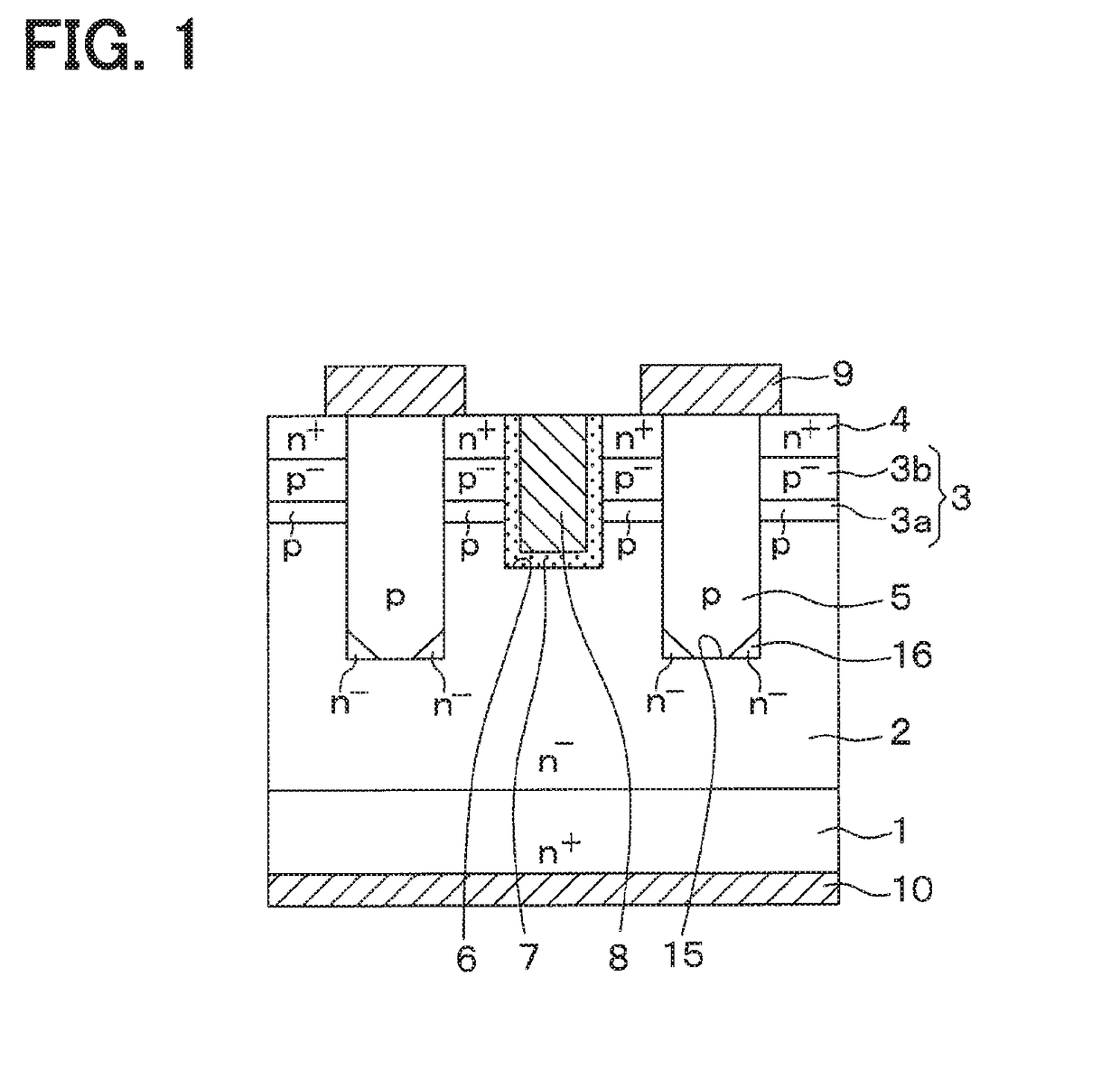
[0021]A SiC semiconductor device according to a first embodiment of the present disclosure in which an inverted vertical MOSFET having a trench gate structure is formed will be described with reference to FIG. 1.

[0022]In the SiC semiconductor device shown in FIG. 1, the vertical MOSFET having the trench gate structure is formed in a cell region, and an outer peripheral high breakdown voltage structure is formed in an outer peripheral region surrounding the cell region.

[0023]The SiC semiconductor device is formed using a semiconductor substrate in which an n−-type drift layer 2 made of SiC having a lower impurity concentration than an n+-type substrate 1 is formed on a front surface side of the n+-type substrate 1 that forms a high concentration impurity layer made of SiC. The n+-type substrate 1 has an n-type impurity concentration of, for example, 1.0×10¹⁹ / cm3 and a front surface of the n+-type substrate 1 is (0001) Si plane. The n−-type drift layer 2 has an n-type impurity concent...

second embodiment

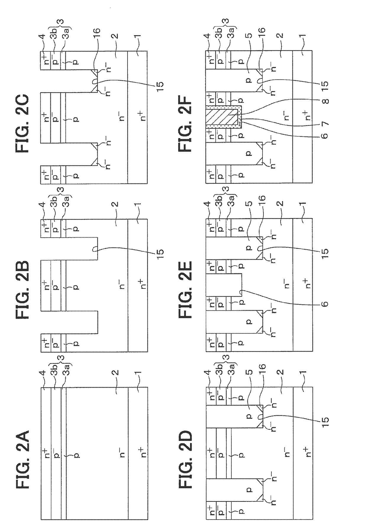
[0058]A second embodiment will be described. In the present embodiment, production processes of the p-type deep layer 5 and the n−-type region 16 are changed with respect to the first embodiment, and others are similar to the first embodiment. Thus, only portions different from the first embodiment will be described.

[0059]In the present embodiment, timings of introducing the dopant gas including the n-type dopant and the dopant gas including the p-type dopant at formation of the p-type deep layer 5 and the n−-type region 16 are changed with respect to the first embodiment.

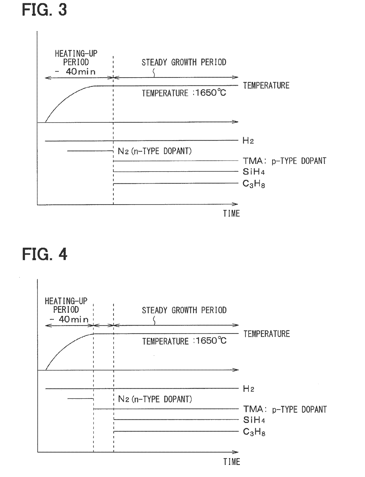
[0060]Specifically, as shown in FIG. 4, the dopant gas including the n-type dopant is introduced in the heating-up period, and after that, before introducing the SiC source gas, the dopant gas including the n-type dopant is switched to the dopant gas including the p-type dopant. Then, after switching of the dopant gas, the introduction of the SiC source gas is performed.

[0061]As described above, the switching of do...

third embodiment

[0064]A third embodiment will be described. In the present embodiment, a configuration of the p-type deep layer 5 is changed with respect to the first embodiment, and others are similar to the first embodiment. Thus, only portions different from the first embodiment will be described.

[0065]As shown in FIG. 6, in the vertical MOSFET provided in the SiC semiconductor device according to the present embodiment, the p-type deep layer 5 has two-layer structure in which the p-type deep layer 5 described in the first embodiment is set as an upper p-type deep layer 5a, and a lower p-type deep layer 5b is provided below the upper p-type deep layer 5a and the n−-type region 16. The lower p-type deep layer 5b is connected with the upper p-type deep layer 5a, and the upper p-type deep layer 5a and the lower p-type deep layer 5b are set to the source potential. A corner portion on a bottom of the lower p-type deep layer 5b has a rounded shape.

[0066]In this way, the p-type deep layer 5b may be re...


PUM


Abstract

A compound semiconductor device includes a semiconductor substrate having a ground layer of a first conductivity type made of a compound semiconductor, a first conductivity type region formed at a corner portion of a bottom of a deep trench formed to the ground layer, and a deep layer of a second conductivity type formed in the deep trench so as to cover the first conductivity type region. A cross section of the first conductivity type region is a triangular shape or a rounded triangular shape in which a portion of the first conductivity type region being in contact with the deep layer is recessed to have a curved surface.

Description

CROSS REFERENCE TO RELATED APPLICATION[0001]This application is based on Japanese Patent Application No. 2016-32292 filed on Feb. 23, 2016, the disclosure of which is incorporated herein by reference.TECHNICAL FIELD[0002]The present disclosure relates to a compound semiconductor device using a compound semiconductor such as silicon carbide (hereafter referred to as SiC) and gallium nitride (hereafter referred to as GaN), and a production method for the same.BACKGROUND ART[0003]Conventionally, Patent Literature 1 proposes a SiC semiconductor device that includes a vertical MOSFET having an inverted trench gate structure as a vertical switching element having a trench gate structure. In the vertical MOSFET having the inverted trench gate structure, a gate voltage is applied to a gate electrode in a gate trench so that a channel is formed in a p-type base region located on a sidewall of the gate trench, and an electric current flows between a drain and a source through the channel. In ...

Claims


Application Information

Patent Timeline
IPC IPC(8): H01L21/266H01L29/78H01L29/423H01L29/16H01L29/20H01L29/66
CPCH01L21/266H01L29/7827H01L29/4236H01L29/66666H01L29/2003H01L29/66068H01L29/1608H01L21/02378H01L21/0243H01L21/02529H01L21/02576H01L21/0262H01L29/7813H01L29/1095H01L29/66734H01L29/872H01L29/0619H01L29/6606H01L21/02639
Inventor TAKEUCHI, YUICHIAKIBA, ATSUYASUZUKI, KATSUMIAOI, SACHIKO
Owner DENSO CORP
Why Eureka
Try Eureka